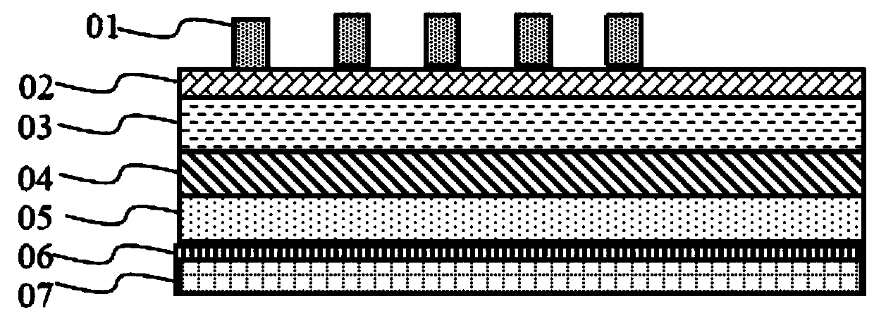
Method for forming mandrel pattern
A mandrel and pattern technology, applied in the manufacture of electrical components, circuits, semiconductor/solid-state devices, etc., can solve the problems of reducing the process window and insufficient protection of the lower film layer, achieve a large process window, reduce the thickness, and solve the mask layer. Insufficient thickness
- Summary
- Abstract
- Description
- Claims
- Application Information
AI Technical Summary
Problems solved by technology
Method used
Image
Examples
Embodiment Construction
[0030] The method for forming the mandrel pattern proposed by the present invention will be further described in detail below in conjunction with the accompanying drawings and specific embodiments. Advantages and features of the present invention will be apparent from the following description and claims. It should be noted that the drawings are all in a very simplified form and use inaccurate scales, and are only used to facilitate and clearly illustrate the purpose of the present invention.
[0031] As device dimensions decrease, critical dimensions in semiconductor manufacturing continue to decrease, even beyond the limits of lithography processes. Under such conditions, in order to obtain structures that can meet critical dimension requirements, self-aligned dual imaging techniques are required. This process first forms the mandrel pattern, forms sidewalls on both sides of the mandrel, and then defines the size of subsequent patterns through the size of the sidewalls. Su...
PUM
 Abstract
Description
Claims
Application Information


