Stacked crimping packaging structure of silicon carbide DSRD

A packaging structure and stacking technology, applied in the field of device packaging, can solve the problems of thermal mismatch partial discharge, unreliability, etc., achieve the effects of reducing electrical connections, improving reliability, and solving reliability problems

Active Publication Date: 2020-07-28
HUAZHONG UNIV OF SCI & TECH
View PDF7 Cites 2 Cited by
  • Summary
  • Abstract
  • Description
  • Claims
  • Application Information

AI Technical Summary

Problems solved by technology

[0006] The present invention provides a silicon carbide DSRD stacked crimping packaging structure, which is used to solve the thermal mismatch and local problems caused by connecting multiple silicon carbide DSRDs end to end through welding in the existing packaging of multiple silicon carbide DSRDs. The unreliable problem of discharge

Method used


Image

  • Stacked crimping packaging structure of silicon carbide DSRD
  • Stacked crimping packaging structure of silicon carbide DSRD
  • Stacked crimping packaging structure of silicon carbide DSRD

Examples


Embodiment 1

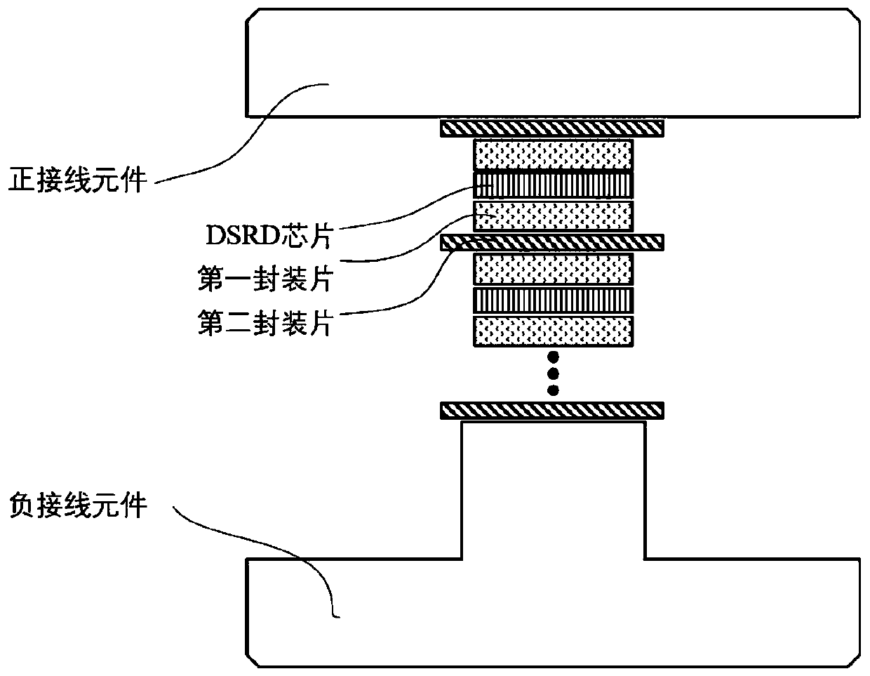
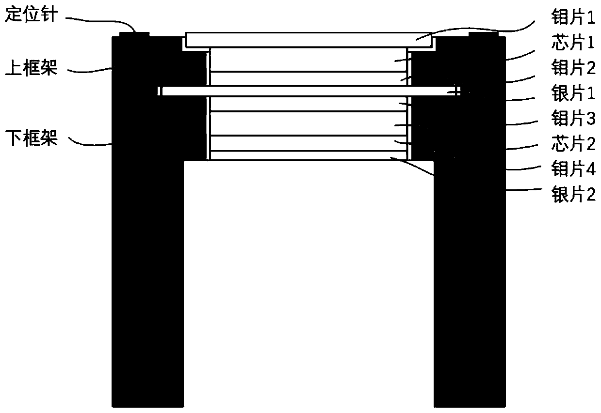
[0033] A stacked press-fit package structure of SiC DSRD, such as figure 1 As shown, it includes: a plurality of first packaging chips, a plurality of second packaging chips, a plurality of DSRD chips, and positive and negative wiring elements.

[0034] Among them, the DSRD chip is a silicon carbide chip, and a layer of first packaging sheets is stacked on both sides of each DSRD chip to form a packaging sub-module; a layer of second packaging sheets is stacked between each adjacent two packaging sub-modules to form a The vertical structure of stacked crimping; in this vertical structure, each adjacent two layers are connected by pressure to realize the electrical connection between each two DSRD chips, and the positive and negative wiring elements are respectively connected to the positive and negative ends of the vertical structure . The material of the first packaging sheet matches the thermal expansion coefficient of the DSRD chip material to avoid thermal deformation cau...


PUM

PropertyMeasurementUnit
thicknessaaaaaaaaaa
thicknessaaaaaaaaaa
lengthaaaaaaaaaa

Abstract

The invention belongs to the field of device packaging and particularly relates to a silicon carbide DSRD stacked crimping packaging structure. The structure comprises a plurality of first packaging sheets, a plurality of second packaging sheets, a plurality of silicon carbide DSRD chips, a positive wiring element and a negative wiring element, wherein a layer of first packaging sheet is stacked on each of two sides of each chip to form a packaging sub-module, every two adjacent packaging sub-modules are stacked through a second packaging sheet to form a stacked crimping vertical structure, every two adjacent layers in the vertical structure are in pressure contact, end-to-end electrical connection between every two chips is achieved, and the positive wiring element and the negative wiringelement are connected with a positive end and a negative end of a vertical structure respectively, the first packaging sheets are used for avoiding thermal deformation caused by thermal mismatch between materials in the working process of the chip, and the second packaging sheets play a role in buffering and are used for realizing optimized modulation of a chip edge electric field. The structureis advantaged in that a vertical stacking crimping form is adopted, so structural installation and failure device replacement are facilitated, a problem of thermal deformation is avoided, electric field modulation is realized, and partial discharge is avoided.

Description

technical field [0001] The invention belongs to the field of device packaging, and more specifically relates to a stacked crimping packaging structure of silicon carbide DSRDs. Background technique [0002] As modern pulse power applications have higher and higher requirements for power devices, in order to simultaneously generate high-voltage and high-speed pulses, DSRD (drift step recovery diode) has been developed in the field of semiconductor pulse power switches. DSRD is a drift step recovery diode, with high withstand voltage, high repetition frequency, and simple structure. The withstand voltage of a single DSRD conventionally produced is mostly under 0.5-2.0kV, and the turn-off time is only 2ns. There is a great development in pulse technology. space. [0003] A high-voltage chip requires a thick epitaxial layer and a deep mesa edge structure, which is difficult to manufacture, and it is difficult for a single DSRD chip to obtain a high breakdown voltage under the r...

Claims


Application Information

Patent Timeline
Patent Type & Authority Applications(China)
IPC IPC(8): H01L25/07H01L23/31H01L23/48H01L23/367H01L23/60
CPCH01L23/3121H01L23/367H01L23/481H01L23/60H01L25/071H01L2224/33181
Inventor 梁琳杨英杰
Owner HUAZHONG UNIV OF SCI & TECH
Why Eureka
Try Eureka