Process for generating multi-step trench transistor by using silicon nitride isolation layer

A trench transistor and isolation layer technology, which is applied in the fields of semiconductor devices, semiconductor/solid-state device manufacturing, electrical components, etc., can solve the problems such as the limited power-on capacity of single-trench transistors and the limited ability to carry high voltages

Active Publication Date: 2020-07-31
绍兴同芯成集成电路有限公司
View PDF5 Cites 0 Cited by
  • Summary
  • Abstract
  • Description
  • Claims
  • Application Information

AI Technical Summary

Problems solved by technology

[0004]Aiming at the deficiencies of the prior art, the purpose of the present invention is to provide a process for forming multi-step trench transistors using silicon nitride isolation layers, which solves the problem of existing The technical problem of the single-trench transistor's limited ability to conduct electricity and the ability to carry high voltage

Method used


Image

  • Process for generating multi-step trench transistor by using silicon nitride isolation layer
  • Process for generating multi-step trench transistor by using silicon nitride isolation layer
  • Process for generating multi-step trench transistor by using silicon nitride isolation layer

Examples


Embodiment Construction

[0030] The following will clearly and completely describe the technical solutions in the embodiments of the present invention with reference to the accompanying drawings in the embodiments of the present invention. Obviously, the described embodiments are only some, not all, embodiments of the present invention. Based on the embodiments of the present invention, all other embodiments obtained by persons of ordinary skill in the art without creative efforts fall within the protection scope of the present invention.

[0031] This embodiment provides a process method for forming a double-trench transistor using a silicon nitride isolation layer, including the following steps:

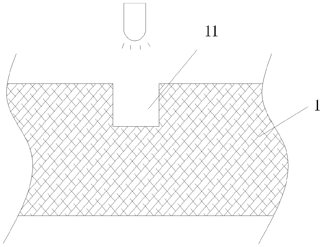
[0032] S1, such as figure 2 As shown, a silicon wafer substrate is selected, and a first trench 11 is etched on the silicon wafer substrate to form a pre-processed transistor 1, and impurities on the side walls of the first trench 11 are cleaned and removed at the same time.

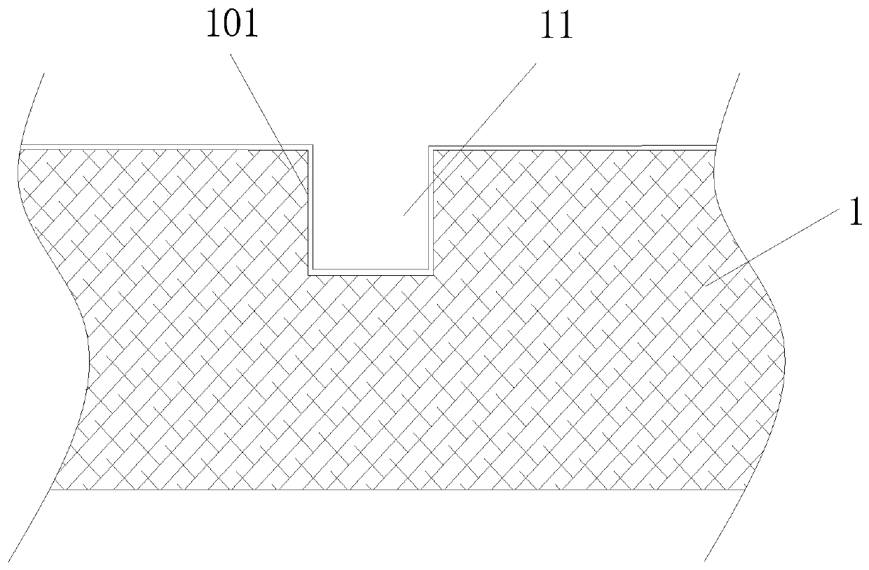
[0033] S2, such as image ...


PUM


Abstract

The invention discloses a process for generating a multi-step trench transistor by using a silicon nitride isolation layer. The process comprises the following steps: S1, etching a first trench on a silicon wafer substrate; S2, placing a primarily processed transistor in an oxidation furnace tube, carrying out oxidation operation, and generating a silicon oxide protective layer on the inner side wall of the first trench; S3, forming a silicon nitride film layer on the silicon oxide protective layer of the first trench through deposition by using a chemical vapor deposition process; S4, carrying out plasma treatment by using fluorine-containing gas to form a side wall; S5, continuously etching the Si layer of the silicon wafer substrate downwards at the bottom of the first trench to form asecond trench; and S6, removing the silicon nitride film layer at the bottom of the first trench by an O2 plasma process to form a double-trench structure. According to the invention, the multi-trenchdesign structure obtains a large transistor area in the same packaging volume, so that the quiescent current passing and high voltage bearing capacities of multiple trenches are increased, and the maximized effective transistor area can be increased by three times.

Description

technical field [0001] The invention belongs to the technical field of wafer production, and in particular relates to a process for forming a multi-step trench transistor by using a silicon nitride isolation layer. Background technique [0002] The semiconductor integrated circuit (IC) industry has undergone rapid development. During the development of ICs, functional density (i.e., the number of interconnected devices per chip area) has generally increased while geometry size (i.e., the smallest device or interconnect line that can be made using a fabrication process) has decreased. The improvement of IC performance is mainly achieved by continuously shrinking the size of integrated circuit devices to increase its speed. The advantages of this scaled-down process are increased production efficiency and reduced associated costs. At the same time, this scaled-down process also increases the complexity of handling and manufacturing ICs. [0003] At present, MOS-FET and IGBT...

Claims


Application Information

Patent Timeline
Patent Type & Authority Applications(China)
IPC IPC(8): H01L21/3065H01L21/306H01L21/308H01L21/336H01L21/331
CPCH01L21/306H01L21/30655H01L21/308H01L29/66325H01L29/66477
Inventor 严立巍陈政勋李景贤
Owner 绍兴同芯成集成电路有限公司
Why Eureka
Try Eureka