Self-supporting gallium nitride single crystal based on HVPE and preparation method thereof

A gallium nitride single crystal, self-supporting technology, applied in the semiconductor field, can solve problems such as the effect of absorbing stress is not very significant, does not reach the heterogeneous substrate, and the process control performance is poor, so as to reduce the nucleation density and improve the crystal Quality, the effect of stress reduction

Inactive Publication Date: 2020-08-07
WUXI WUYUE SEMICON CO LTD
View PDF4 Cites 2 Cited by
  • Summary
  • Abstract
  • Description
  • Claims
  • Application Information

AI Technical Summary

Problems solved by technology

[0005] However, such methods have disadvantages: 1. High cost, requiring expensive equipment and index processes such as lithography machines or MOCVD; 2. Additional equipment and processes are required, resulting in poor process control performance and reduced yield; 3. Absorbing stress The effect is not very significant
At present, the largest GaN self-supporting substrate in the industry is about 4 inches, which is far from reaching the size of heterogeneous substrates such as silicon, sapphire, and silicon carbide, such as 8 inches or even larger.

Method used


Image

  • Self-supporting gallium nitride single crystal based on HVPE and preparation method thereof
  • Self-supporting gallium nitride single crystal based on HVPE and preparation method thereof
  • Self-supporting gallium nitride single crystal based on HVPE and preparation method thereof

Examples


Embodiment 1

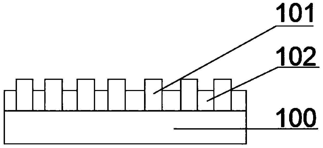
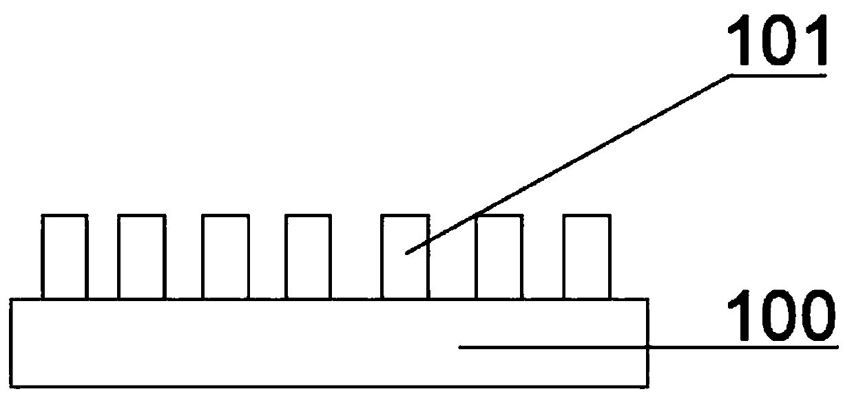
[0041] according to Figure 1-5 , the present invention provides a self-supporting gallium nitride single crystal based on HVPE, the preparation method of the self-supporting gallium nitride single crystal based on HVPE comprises the following steps:

[0042] (1) Provide a substrate, and perform cleaning and nitriding treatment on the surface of the substrate.

[0043] (2) growing GaN crystal nuclei on the surface of the substrate at low temperature, while HCl and NH3 form NH4Cl solids, competing with GaN crystal nuclei to cover the substrate;

[0044] (3) The temperature is increased to above 1000°C for annealing treatment to improve the quality of GaN crystal nuclei;

[0045] (4) two-dimensionally growing a GaN layer on the GaN crystal nucleus at medium and high temperature;

[0046] (5) Continuously growing a GaN single crystal at high temperature on the GaN layer;

[0047] (6) Lowering the temperature and peeling off the GaN single crystal from the substrate to form a s...

Embodiment 2

[0058] The HVPE-based self-supporting gallium nitride single crystal provided in this example is roughly the same as the method provided in Example 1, except that the low temperature range of step (2) is 370-440°C, V / III is 200, The coverage rate of the GaN crystal nucleus is 56%, and its growth thickness is 60-80nm.

[0059] As a preferred setting of the embodiment of the present invention, the GaN layer in step (4) is two-dimensionally grown at a medium and high temperature of 800-1100°C, V / III is set to 10, the growth rate is 20um / hr, and the thickness is 8-10um.

[0060] In addition, the technical features disclosed in Embodiment 1 are also applicable to this embodiment, and other technical features already disclosed in Embodiment 1 will not be repeated here.

Embodiment 3

[0062] The HVPE-based self-supporting gallium nitride single crystal provided in this example is roughly the same as the method provided in Example 1, except that the low temperature range of step (2) is 440-500°C, V / III is 200, The coverage rate of the GaN crystal nucleus is 65%, and its growth thickness is 70-100nm.

[0063] As a preferred setting of the embodiment of the present invention, the GaN layer in step (4) is two-dimensionally grown at a medium and high temperature of 950-1100°C, V / III is set to 20, the growth rate is 30um / hr, and the thickness is 6-10um.


PUM

PropertyMeasurementUnit
thicknessaaaaaaaaaa
thicknessaaaaaaaaaa
thicknessaaaaaaaaaa

Abstract

The invention provides a preparation method of a self-supporting gallium nitride single crystal based on HVPE, and the method comprises the following steps: (1) providing a substrate, and carrying outthe in-situ cleaning of the surface of the substrate; (2) growing a GaN crystal nucleus on the surface of the substrate at a low temperature, and forming NH4Cl solid from HCl and NH3 at the same timeto compete with the GaN crystal nucleus to cover the substrate; (3) increasing the temperature to 1000 DEG C or above for annealing treatment, and improving the GaN crystal nucleus quality; (4) growing a GaN layer on the GaN crystal nucleus in a medium-high temperature two-dimensional manner; and (5) continuously growing GaN single crystals on the GaN layer at a high temperature; and cooling, andstripping the GaN single crystal from the substrate to form the self-supporting crystal. High-quality nucleation points are provided for growth of self-supporting gallium nitride through HVPE, warping is reduced due to the fact that gaps release stress, cracking is eliminated when growth is finished and cooling is conducted, and the growth yield of the self-supporting gallium nitride is increased.

Description

technical field [0001] The invention relates to the technical field of semiconductors, in particular to a self-supporting gallium nitride single crystal and a preparation method thereof. Background technique [0002] GaN is a typical representative of the third-generation wide-bandgap semiconductors. It has been widely used in semiconductor lighting, microwave power devices, and power electronic devices, showing great application prospects. The most ideal substrate for gallium nitride growth is naturally gallium nitride single crystal material. Such homoepitaxial (that is, the epitaxial layer and the substrate are the same material) can greatly improve the crystal quality of the epitaxial film and reduce the dislocation density. , Improve the working life of the device, improve the luminous efficiency, and increase the working current density of the device. However, gallium nitride single crystal growth is difficult and expensive, and large-scale homoepitaxial growth is sti...

Claims


Application Information

Patent Timeline
Patent Type & Authority Applications(China)
IPC IPC(8): C30B29/40C30B25/18C30B33/02
CPCC30B25/025C30B25/183C30B25/186C30B29/406C30B33/02
Inventor 刘良宏庞博许彬张海涛
Owner WUXI WUYUE SEMICON CO LTD
Why Eureka
Try Eureka