

Through hole electroplating process for printed circuit board
A printed circuit board and through-hole electroplating technology, applied in the electrolysis process, electrolysis components, cells, etc., can solve the problems of insufficient copper thickness in the hole, poor through-hole, uneven copper thickness from top to bottom, etc., to improve the electroplating effect, The effect of reducing plating time and increasing plating thickness
- Summary
- Abstract
- Description
- Claims
- Application Information
AI Technical Summary
Problems solved by technology
Method used
Image

Examples
Embodiment 1
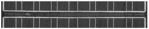
[0056] Test sample: 10mm printed circuit board, the diameter of the through hole is 0.3mm.
[0057] Degreasing: Use the acid degreasing agent model 717 of MacDermid Technology (Suzhou) Co., Ltd. to degrease the printed circuit board. The operating temperature of degreasing is 54 ° C and the time is 3 minutes.
[0058] The operating concentration of the degreasing agent is 12%, and the solvent is deionized water.
[0059] Water washing: the printed circuit board was washed with flowing deionized water and mechanical shaking, the operating temperature of water washing was 25° C., and the washing time was 3 minutes.
[0060] It can be understood that the function of water washing is mainly to remove the acid degreaser on the printed circuit board, so as not to contaminate the subsequent potion.
[0061] Pre-soaking: the printed circuit board is pre-soaked using 10% sulfuric acid solution combined with a mechanical shaking and filtration circulation system. The operating temperat...
Embodiment 2
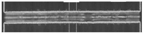
[0074] Test sample: 4.5mm printed circuit board with a through hole diameter of 0.2mm.
[0075] Degreasing: Use the acid degreasing agent model 717 of MacDermid Technology (Suzhou) Co., Ltd. to degrease the printed circuit board. The operating temperature of degreasing is 54 ° C and the time is 3 minutes.
[0076] The operating concentration of the degreasing agent is 12%, and the solvent is deionized water.
[0077] Water washing: the printed circuit board was washed with flowing deionized water and mechanical shaking, the operating temperature of water washing was 25° C., and the washing time was 3 minutes.
[0078] It can be understood that the function of water washing is mainly to remove the acid degreaser on the printed circuit board, so as to avoid subsequent contamination of subsequent potions.
[0079] Pre-soaking: the printed circuit board is pre-soaked using 10% sulfuric acid solution combined with a mechanical shaking and filtration circulation system. The operati...
Embodiment 3
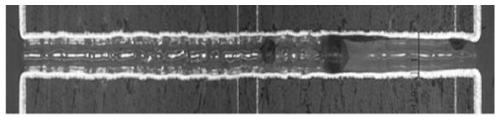
[0093] Test sample: 4.5mm printed circuit board, the hole diameter of the through hole is 0.25mm.
[0094] Degreasing: Use the acid degreasing agent model 717 of MacDermid Technology (Suzhou) Co., Ltd. to degrease the printed circuit board. The operating temperature of degreasing is 54 ° C and the time is 3 minutes.
[0095] The operating concentration of the degreasing agent is 12%, and the solvent is deionized water.
[0096] Water washing: the printed circuit board was washed with flowing deionized water and mechanical shaking, the operating temperature of water washing was 25° C., and the washing time was 3 minutes.
[0097] It can be understood that the function of water washing is mainly to remove the acid degreaser on the printed circuit board, so as to avoid subsequent contamination of subsequent potions.
[0098] Pre-soaking: the printed circuit board is pre-soaked using 10% sulfuric acid solution combined with a mechanical shaking and filtration circulation system. ...
PUM
| Property | Measurement | Unit |
|---|---|---|
| thickness | aaaaa | aaaaa |
| thickness | aaaaa | aaaaa |
| thickness | aaaaa | aaaaa |
Abstract
Description
Claims
Application Information