Multi-level shift circuit based on composite dielectric gate double-transistor photosensitive detector

A technology of photosensitive detectors and dual transistors, which is applied in the direction of logic circuit coupling/interfaces, circuits, and electric solid-state devices using field effect transistors. The effect of sexual dominance

Active Publication Date: 2020-08-14
NANJING UNIV
View PDF8 Cites 1 Cited by
  • Summary
  • Abstract
  • Description
  • Claims
  • Application Information

AI Technical Summary

Problems solved by technology

[0004] The traditional level shifting circuit only supports the shifting and switching of single-level signals or dual-level models, which cannot meet the requirements of the positive pressure, negative voltage, zero level and floating four signals required by the composite dielectric grating photosensitive detector. Two switches, so it is necessary to design a multi-level shift circuit for composite dielectric gate dual-transistor photosensitive detectors

Method used


Image

  • Multi-level shift circuit based on composite dielectric gate double-transistor photosensitive detector
  • Multi-level shift circuit based on composite dielectric gate double-transistor photosensitive detector
  • Multi-level shift circuit based on composite dielectric gate double-transistor photosensitive detector

Examples


Embodiment 1

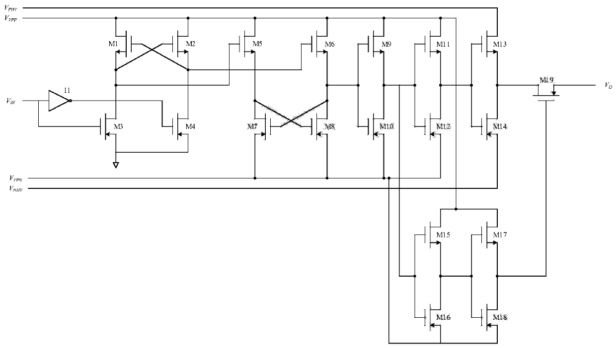
[0032] In this embodiment, a multi-level shift circuit is provided, such as image 3 shown. Among them, I1 and M1~M8 constitute a pre-shift circuit, M9~M12 are drive circuits, M13 and M14 are shift circuits, M15~M19 are signal compensation circuits, and the gray part is a deep N well. The specific circuit is as follows: the pre-shift control signal V IN Connect the gate terminal of transistor M3 and the input terminal of inverter I1, the output terminal of inverter I1 is connected to the gate terminal of transistor M4, the source terminals of transistors M3 and M4 are both grounded; the drain terminal of transistor M3 is connected to the source terminal of transistor M1 , the gate terminals of the transistor M2 and the transistor M5, the drain terminal of the transistor M4 is connected to the source terminal of the transistor M2, the gate terminal of the transistor M1 and the gate terminal of the crystal M6, and the drain terminals of the transistors M1, M2, M5, and M6 are al...

Embodiment 2

[0035] In this embodiment, the above-mentioned multi-level shift circuit is used to drive the composite dielectric gate double-transistor photosensitive detector pixel, such as Figure 4 shown. C1, C2, and M0 constitute a composite dielectric gate double-transistor photosensitive detector, the gray part is a deep N well, and the outputs of multi-level conversion circuits #1, #2, #3, #4, and #5 are respectively connected to the composite dielectric The gate, drain, substrate, source, and deep N-well of the gate double-transistor photosensitive detector provide driving voltages for them.

Embodiment 3

[0037] In this embodiment, the above-mentioned multi-level shift circuit is used to drive a composite dielectric gate double-transistor photosensitive detector array, such as Figure 5 shown. The photosensitive detector array has 2 rows and 2 columns. The gate ends of the composite dielectric gate double transistor photosensitive detectors of each row are connected to form a word line, the drain terminals are connected to form a bit line, and the source terminals are connected to form a source line; all the substrates of the composite dielectric gate double transistor photosensitive detectors are connected to form a substrate, Placed in a deep N well (gray area in the figure). The outputs of multi-level conversion circuits #1 and #2 are respectively connected to the word line of the composite dielectric gate double transistor photosensitive detector array to provide driving voltage; the outputs of multi-level conversion circuits #3 and #4 are respectively connected to the com...


PUM


Abstract

The invention discloses a multi-level shift circuit based on a composite dielectric gate double-transistor photosensitive detector. The detector unit comprises an MOS-C (Metal Oxide Semiconductor) part and an MOSFET (Metal Oxide Semiconductor Field Effect Transistor) part; five ports of an N-type source region, an N-type drain region, a second control gate, a P-type semiconductor substrate and anN-type trap of the unit are respectively connected with a multi-level shift circuit, and the shift circuit comprises a pre-shift circuit, a shift circuit, a drive circuit and a signal compensation circuit. According to the shift circuit, pairwise switching of the positive voltage signal, the negative voltage signal, the zero potential signal and the floating signal can be achieved in one circuit,and compared with a traditional level shift circuit only supporting a single voltage signal or double voltage signals, the shift circuit has more advantages in the aspects of power consumption, performance, compatibility and the like.

Description

technical field [0001] The invention relates to a multi-level shift circuit based on a compound dielectric gate dual-transistor photosensitive detector, which belongs to the field of integrated circuits. Background technique [0002] CCD and CMOS-APS, as the two most common imaging devices at present, have their own limitations. Due to the complex control timing and voltage requirements of CCD, the working speed is slow and it is not easy to integrate; CMOS-APS uses photosensitive diodes and has a complex structure, resulting in low fill factor and small full well charge. [0003] In the existing patent CN201210442007.X, a dual-transistor photosensitive detector is proposed. The feature of this sensor is that a single semiconductor device can realize complete reset, light-sensing and readout functions, thus forming a complete pixel, which can be extremely Greatly increases the fill factor of pixels. As a new generation of imaging device, composite dielectric gate dual-tran...

Claims


Application Information

Patent Timeline
Patent Type & Authority Applications(China)
IPC IPC(8): H03K19/0185H01L27/146H01L29/423
CPCH03K19/0185H01L27/14614H01L29/42364
Inventor 闫锋王凯沈凡翔柴智胡心怡顾郅扬吴天泽
Owner NANJING UNIV
Why Eureka
Try Eureka