Parameter design method of phase-shifted full-bridge converter based on ZVS load range
A technology of phase-shifting full bridge and parameter design, applied in design optimization/simulation, output power conversion device, conversion of DC power input to DC power output, etc.
- Summary
- Abstract
- Description
- Claims
- Application Information
AI Technical Summary
Problems solved by technology
Method used
Image
Examples
Embodiment Construction
[0036] Specific embodiments of the present invention will be further described below in conjunction with the accompanying drawings.
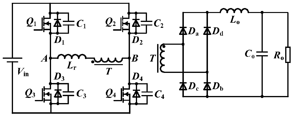
[0037] refer to figure 1 Shown is the basic topology of the main circuit of the ZVS phase-shifted full-bridge DC-DC converter, where Q1 and Q3 are leading transistors, Q2 and Q4 are lagging transistors, D1~D4 are switching body diodes, and C1~C4 are switching diodes. Tube parallel resonant capacitor, Lr is resonant inductance (including leakage inductance of high frequency transformer), T is high frequency transformer, Da, Db, Dc, Dd are secondary side rectifier diodes, L 0 is the output filter inductor, C 0 is the output filter capacitor, R 0 for the load. The leading arms Q1 and Q3 are respectively ahead of the lagging arms Q2 and Q4 by a phase shift angle, and the output voltage is adjusted by changing the magnitude of the phase shift angle. Assuming that the inductors, power transformers, power switches, diodes and other components in th...
PUM
 Abstract
Description
Claims
Application Information


