Correction method suitable for two-step ADC

A correction method and slope technology, applied in analog/digital conversion calibration/testing, signal transmission systems, instruments, etc., can solve problems such as overall accuracy impact, voltage reduction, and impact on the correctness of quantization results.

Active Publication Date: 2020-08-21
UNIV OF ELECTRONICS SCI & TECH OF CHINA
View PDF13 Cites 11 Cited by
  • Summary
  • Abstract
  • Description
  • Claims
  • Application Information

AI Technical Summary

Problems solved by technology

as attached figure 2 Shown is a schematic diagram of the comparison between the ideally loaded rough ramp step voltage and the actually loaded rough ramp step voltage, where V FB , V FT In order to generate the minimum value and maximum value of the rough ramp voltage, it is the quantization range of the rough ramp. With the continuous increase of the rough ramp voltage code value, the voltage actually loaded on the capacitor after the rough quantization is greatly reduced, and the overall linearity is seriously affected. influences
Further consideration, when the code value is large, the gap between the voltage loaded on the capacitor and the ideal situation is above the 1LSB voltage of the thick slope, resulting in insufficient quantization interval of the fine slope to complete the quantization, which seriously affects the overall accuracy
[0017] It can be seen that due to the nonlinear parasitic capacitance of the device and the influence of switch charge injection in the two-step single-slope ADC, there will be a large gap between the actual quantized output result and the theoretical design value, which will affect the correctness of the quantized result, and ultimately make the analog-to-digital conversion Various performance indicators of the converter are difficult to meet the requirements, including integral nonlinearity (INL), differential nonlinearity (DNL), spurious-free dynamic range (SFDR), etc.

Method used


Image

  • Correction method suitable for two-step ADC
  • Correction method suitable for two-step ADC
  • Correction method suitable for two-step ADC

Examples


Embodiment Construction

[0060] The technical solution of the present invention will be further described through the embodiments below in conjunction with the accompanying drawings.

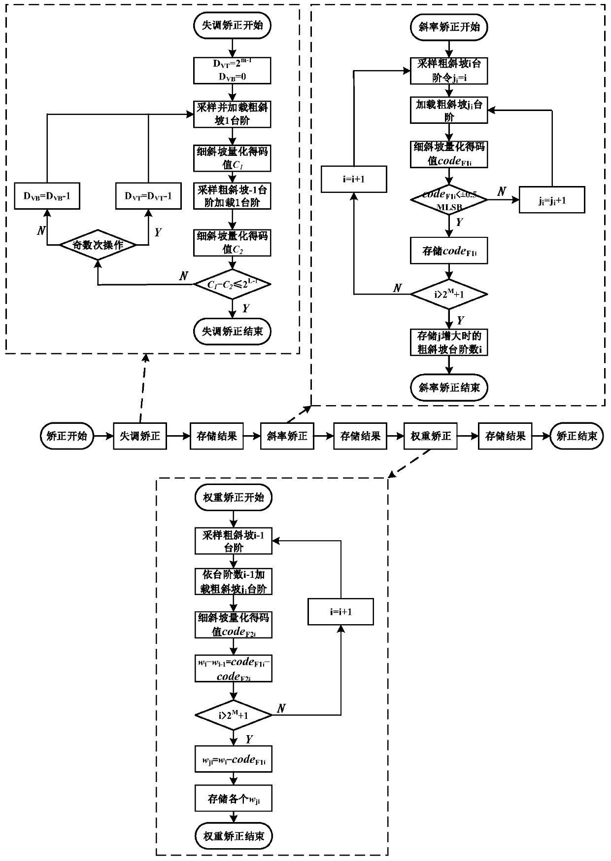
[0061] Such as image 3 Shown is a logic block diagram of a correction method suitable for two-step ADC proposed by the present invention. The correction method proposed by the present invention works before the normal quantization of the two-step ADC, including correcting fine slope clamping operational amplifier offset, correcting There are three parts of coarse slope slope and corrected coarse slope weight, including the following steps:

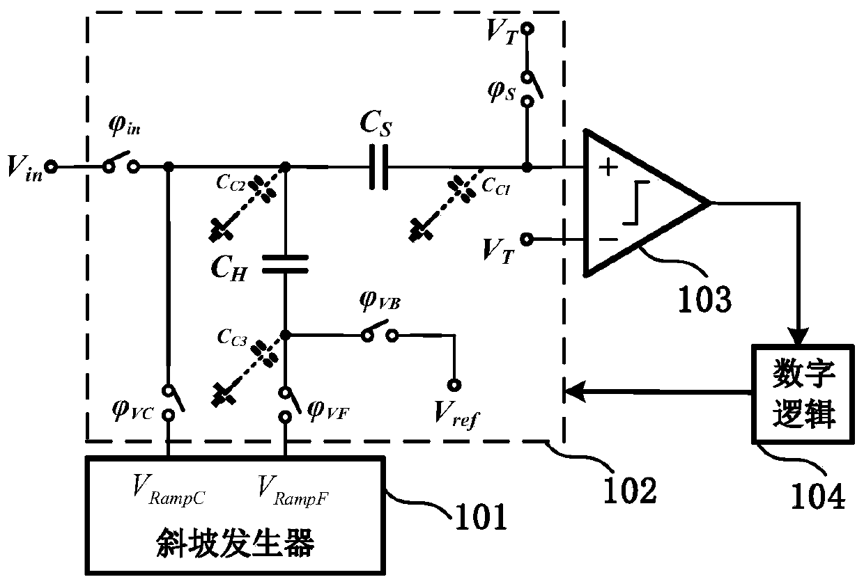
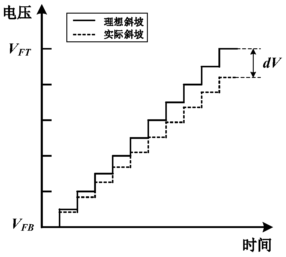
[0062] Step 1. Before the quantization of the two-step ADC starts, correct the offset of the clamping op-amp of the thin ramp generating unit. Such as Figure 4 Shown is a schematic circuit diagram of the ramp generator, including a thick ramp generating unit 401 and a fine ramp generating unit 402, wherein the thick ramp completes the quantization of the high M bits, the fine ra...


PUM


Abstract

The invention relates to a correction method suitable for a two-step ADC, and the method comprises the following steps: when the two-step ADC performs normal quantization, firstly correcting the clamping operational amplifier imbalance of a fine slope to eliminate the influence of the imbalance on the linearity; correcting the slope and the weight value of the step voltage of the coarse slope by utilizing the fine slope; through delaying the disconnection time of the third switch after the coarse slope quantization is finished, enabling the coarse slope to continuously rise after the quantization is finished; enabling the voltage loaded on the capacitor to be close to an ideal voltage, and further quantifying the actual voltage weight loaded on the capacitor by the coarse slope; compensating for the voltage attenuation caused by capacitor parasitism and other factors by delaying the coarse slope for a corresponding period number, so the linearity of the system is greatly improved, andthe precision of the ADC is improved. During normal quantization, only delay processing needs to be carried out on an original coarse slope, no extra analog device is introduced, and the overall circuit area is not greatly affected.

Description

technical field [0001] The invention belongs to the technical field of analog-to-digital conversion, and in particular relates to a correction method suitable for a two-step ADC. Background technique [0002] With the rapid development of the field of integrated circuits, the integration of integrated circuits is getting higher and higher, requiring higher precision and higher density for circuit design. In the communication industry, under the background of continuous attention and rapid development in the field of image processing and environmental monitoring, the analog-to-digital converter (ADC) as the interface for converting digital information and analog information has become particularly important. This requires the analog-to-digital converter to achieve higher speed and achieve higher precision. In the actual analog-to-digital converter circuit, in addition to requiring as low power consumption as possible, low integral nonlinearity (INL), low differential nonline...

Claims


Application Information

Patent Timeline
Patent Type & Authority Applications(China)
IPC IPC(8): H03M1/10H03M1/50
CPCH03M1/1009H03M1/50
Inventor 宁宁孟昊邓恒张启辉李靖于奇
Owner UNIV OF ELECTRONICS SCI & TECH OF CHINA
Why Eureka
Try Eureka