Light-emitting diode with hole injection structure electron blocking layer

A technology of light-emitting diodes and hole injection layers, applied in circuits, electrical components, semiconductor devices, etc., can solve the problems of low carrier recombination efficiency and luminous efficiency, reduced hole injection efficiency, and reduced LED luminous efficiency, etc., to achieve Effects of improving vertical migration ability, suppressing leakage, and improving hole injection efficiency

Active Publication Date: 2020-08-28
SOUTHEAST UNIV
View PDF10 Cites 9 Cited by
  • Summary
  • Abstract
  • Description
  • Claims
  • Application Information

AI Technical Summary

Problems solved by technology

The electron blocking layer adopting the above-mentioned structures still cannot solve the following technical problems: In order to obtain a suitable hole concentration, it is often necessary to increase the doping concentration of Mg atoms, which will inevitably make the Mg atoms in the traditional P-type superlattice structure electron blocking layer diffuse. Entering the active area, it becomes a non-radiative recombination center, which further reduces the luminous efficiency of the LED; the electron blocking layer with high Al composition has a significant blocking effect on electrons and holes, resulting in a significant decrease in the injection efficiency of holes, resulting in the LED's Carrier recombination efficiency and luminous efficiency are still low

Method used


Image

  • Light-emitting diode with hole injection structure electron blocking layer
  • Light-emitting diode with hole injection structure electron blocking layer
  • Light-emitting diode with hole injection structure electron blocking layer

Examples


Embodiment Construction

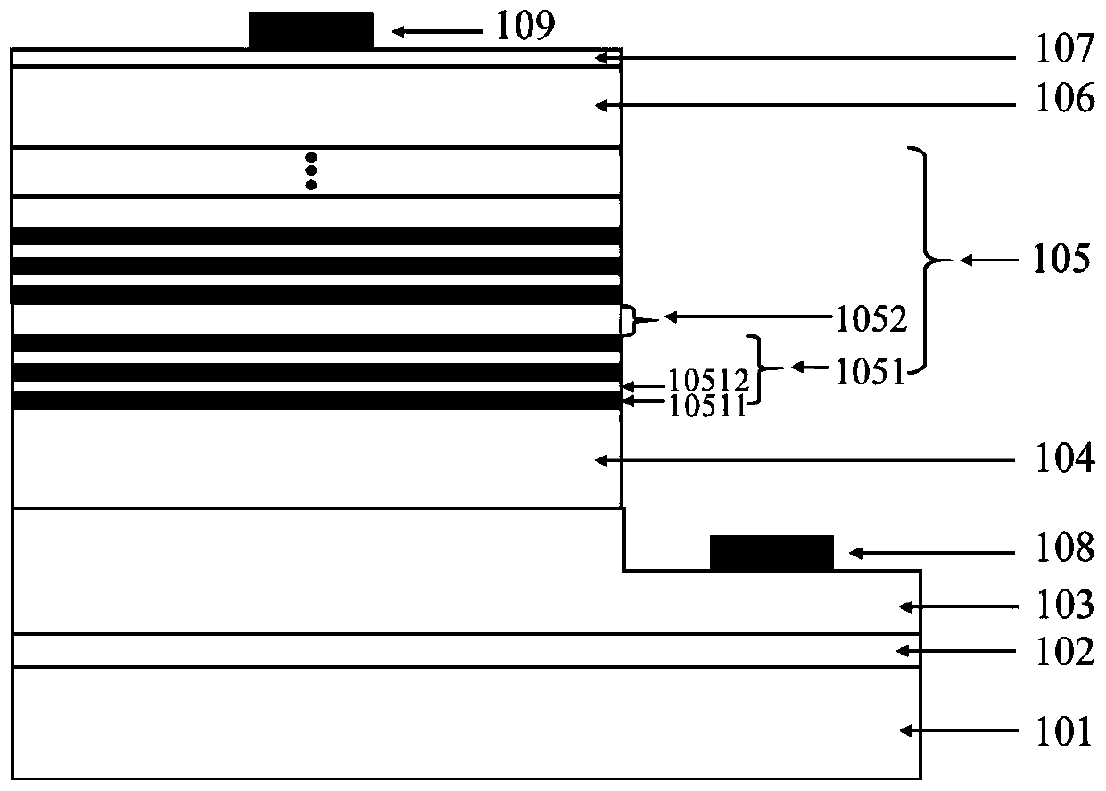
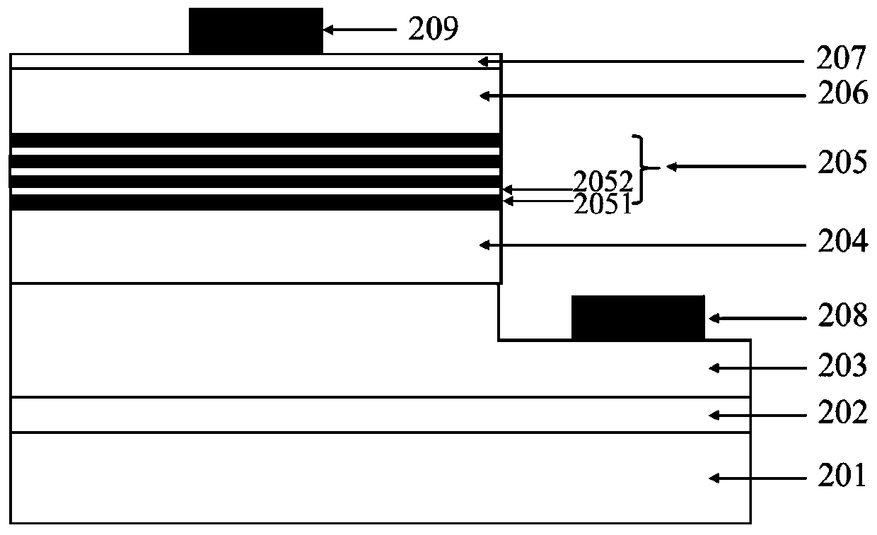
[0027] Such as figure 1 , a light-emitting diode with a hole injection structure electron blocking layer of the present invention, comprising: a sapphire substrate 101, a GaN buffer layer 102, an n-type GaN layer 103, a GaN / In 0.3 Ga 0.7 N multi-quantum well active region 104, hole injection structure electron blocking layer 105, p-type GaN layer 106, transparent conductive layer 107, also includes the n-type ohmic electrode 108 that is arranged on the n-type GaN layer 103, and is arranged on the transparent A p-type ohmic electrode 109 on the conductive layer 107 .

[0028] The thickness of the GaN buffer layer 102 is 30 nm; the thickness of the n-type GaN layer 103 is 3 μm; GaN / In 0.2 Ga 0.8 The N multi-quantum well active region 104 has 8 pairs of quantum wells, In 0.2 Ga 0.8 The well thickness of the N quantum well is 3nm, and the thickness of the GaN barrier is 10nm; the total thickness of the electron blocking layer of the hole injection structure is 45nm; the thic...


PUM

PropertyMeasurementUnit
thicknessaaaaaaaaaa
thicknessaaaaaaaaaa
thicknessaaaaaaaaaa

Abstract

The invention discloses a light-emitting diode with an electron blocking layer of a hole injection structure. The light-emitting diode comprises a substrate, a nitride buffer layer, an n-type nitridelayer, a multi-quantum well active region, a hole injection structure electron blocking layer, a p-type nitride layer and a transparent conductive layer which are sequentially arranged from bottom totop, and further comprises an n-type electrode arranged on the n-type nitride layer and a p-type electrode arranged on the transparent conductive layer. According to the light-emitting diode of the electron blocking layer of the hole injection structure, stress matching between the active region and the electron blocking layer is achieved, electron leakage is effectively restrained. Meanwhile, theprobability that Mg diffuses into the active region is reduced, and then the light-emitting efficiency of the LED is improved; the longitudinal migration capability of holes is improved, so that thehole injection efficiency is remarkably improved; the polarized electric field at the heterojunction interface forms two-dimensional hole gas on one side of the hole injection layer, so that the congestion effect of current is improved.

Description

technical field [0001] The invention relates to the manufacturing field of semiconductor optoelectronic materials and devices, in particular to a light-emitting diode with an electron blocking layer of a hole injection structure. Background technique [0002] Due to its advantages of high efficiency, energy saving, small size, and strong controllability of the light-emitting band, LEDs are widely used in the fields of outdoor display screens, TV backlights, and lighting lamps. However, with the increase of operating current, LED luminous efficiency rapidly This problem seriously restricts the application and development of LEDs. Research results in recent years have shown that carrier leakage is one of the key factors leading to the decline in luminous efficiency of LEDs injected with large currents. In order to effectively block the overflow of electrons, researchers have theoretically and experimentally confirmed that the traditional single-layer P-AlGaN in GaN-based LEDs ...

Claims


Application Information

Patent Timeline
Patent Type & Authority Applications(China)
IPC IPC(8): H01L33/14H01L33/04H01L33/06
CPCH01L33/14H01L33/145H01L33/04H01L33/06
Inventor 张雄沈阳胡国华崔一平
Owner SOUTHEAST UNIV
Why Eureka
Try Eureka