Monocrystalline silicon wafer cleaning method
A single crystal silicon wafer, silicon wafer technology, applied in sustainable manufacturing/processing, electrical components, climate sustainability, etc., can solve the problem that the cleaning process cannot be applied to single crystal silicon wafer cleaning
- Summary
- Abstract
- Description
- Claims
- Application Information
AI Technical Summary
Problems solved by technology
Method used
Image

Examples
Embodiment 1
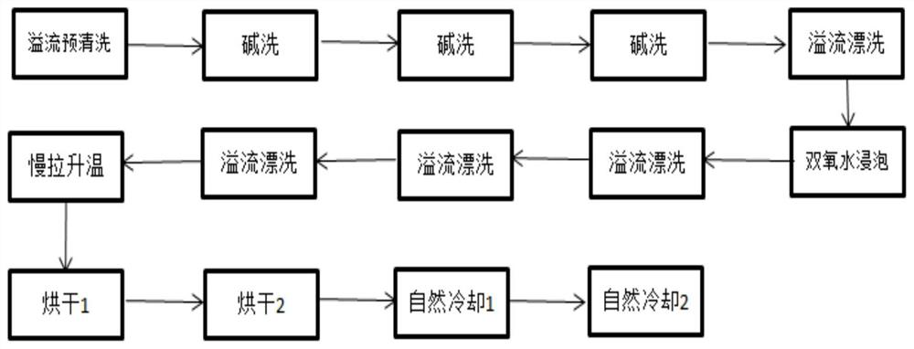
[0020] Such as figure 1 As shown, the monocrystalline silicon wafer cleaning method of the present invention sequentially includes the steps of overflow pre-cleaning, alkali cleaning, primary overflow rinsing, hydrogen peroxide soaking, secondary overflow rinsing, slow heating, drying, and natural cooling at room temperature, specifically as follows:
[0021] Overflow pre-cleaning: The overflow speed of single crystal is required to be 220L / Hour. The function is to pre-clean the surface of the silicon wafer after degumming, and simply remove large impurities on the surface of the silicon wafer such as glue, degumming agent, and lactic acid;
[0022] Alkali cleaning: Use solid alkali (purified grade KOH), surfactant, and pure water to prepare an alkaline cleaning mixed solution (KOH) with a concentration of 3%, and use three ultrasonic alkaline cleaning tanks to clean the silicon wafers in sequence. 50°C;
[0023] One overflow rinse: overflow speed 300L / Hour. The function is...
Embodiment 2
[0030] The cleaning method of monocrystalline silicon wafers includes pre-cleaning, alkaline cleaning, primary overflow rinsing, hydrogen peroxide immersion, secondary overflow rinsing, slow heating, drying, and natural cooling at room temperature. The details are as follows:
[0031] Overflow pre-cleaning: The overflow speed of single crystal is required to be 250L / Hour. The function is to pre-clean the surface of the silicon wafer after degumming, and simply remove residual substances such as glue, degumming agent, lactic acid, etc.;
[0032] Alkali cleaning: Use solid alkali (purified grade KOH), surfactant, and pure water to prepare an alkaline cleaning mixed solution (KOH) with a concentration of 4%, and use three ultrasonic alkaline cleaning tanks to clean the silicon wafers in sequence. 55°C;
[0033] One-time overflow rinsing: the overflow speed is 210L / Hour. The function is to rinse the mixed solution (KOH / surfactant) after alkali washing to reduce the chemical resid...
Embodiment 3
[0040] The cleaning method of monocrystalline silicon wafers includes pre-cleaning, alkaline cleaning, primary overflow rinsing, hydrogen peroxide immersion, secondary overflow rinsing, slow heating, drying, and natural cooling at room temperature. The details are as follows:
[0041] Overflow pre-cleaning: the overflow speed of single crystal is required to be 230L / Hour. The function is to pre-clean the surface of the silicon wafer after degumming, and simply remove residual substances such as glue, degumming agent, lactic acid, etc.;
[0042] Alkali cleaning: Use solid alkali (purified grade KOH), surfactant, and pure water to prepare an alkaline cleaning mixed solution (KOH) with a concentration of 5%, and use multiple ultrasonic alkaline cleaning tanks to clean the silicon wafers in sequence. The temperature requirement is at 60°C;
[0043] One-time overflow rinsing: the overflow speed is 350L / Hour. The function is to rinse the mixed solution (KOH / surfactant) after alkali...
PUM
 Abstract
Description
Claims
Application Information
 - R&D Engineer
- R&D Manager
- IP Professional
- Industry Leading Data Capabilities
- Powerful AI technology
- Patent DNA Extraction
Browse by: Latest US Patents, China's latest patents, Technical Efficacy Thesaurus, Application Domain, Technology Topic.
© 2024 PatSnap. All rights reserved.Legal|Privacy policy|Modern Slavery Act Transparency Statement|Sitemap