

Manufacturing method of electromagnetic shielding material, electromagnetic shielding material and electronic product
A technology of electromagnetic shielding material and manufacturing method, applied in magnetic field/electric field shielding, metal material coating process, electrical components, etc., can solve the problems of difficult to thin conductive cloth, high cost, large environmental pollution, etc. Effect and flexibility of use, boosting energy, simple process effect
- Summary
- Abstract
- Description
- Claims
- Application Information
AI Technical Summary
Problems solved by technology
Method used
Image

Examples
Embodiment 1
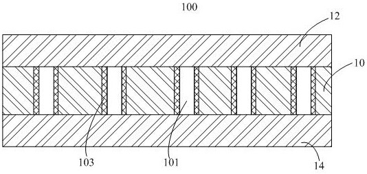
[0045] A polymer film layer is provided, the thickness of the polymer film layer is 1.5 microns, and the material is polyethylene terephthalate.
[0046] A polymer film layer is provided, the thickness of the polymer film layer is 1.5 microns, and the material is polyethylene terephthalate.
[0047] The polymer film layer is baked at a temperature of 45 degrees centigrade for 24 hours.
[0048] Carry out laser drilling to the polymer film layer that is processed through baking, make polymer film layer form several through holes, the aperture of some through holes is 0.1 micron, and the pitch is 0.1 micron, and the shape of several through holes is circular.
[0049] Carry out corona treatment to two surfaces of the polymer film layer after punching, and the corona treatment time is 1 second. The dyne value of both surfaces after corona treatment was 56.
[0050] A layer of metal shielding layer is respectively sputtered on the two surfaces of the polymer film layer after cor...
Embodiment 2
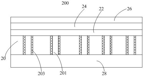
[0053] A polymer film layer is provided, the thickness of the polymer film layer is 6 microns, and the material is polycarbonate.
[0054] The polymer film layer is baked at a temperature of 80 degrees centigrade for 1 hour.
[0055] Carry out laser drilling to the polymer film layer that is processed through baking, make polymer film layer form some through holes, the aperture of some through holes is 100 microns, and the pitch is 100 microns. Some of the through holes are triangular in shape.
[0056] Carry out corona treatment to the two surfaces of the polymer film layer after punching, and the corona treatment time is 10 seconds respectively. The dyne value of both surfaces after corona treatment was 54.
[0057] The first layer of metal shielding layer is sputtered on the two surfaces of the polymer film layer after corona treatment and the hole walls of several through holes, with zinc as the target material, and continuous winding coating is adopted. The coating proc...
Embodiment 3
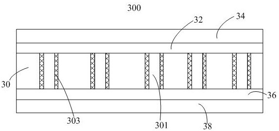
[0060] A polymer film layer is provided, the thickness of the polymer film layer is 2 microns, and the material is polypropylene.
[0061] Laser drilling is carried out to the polymer film layer, so that the polymer film layer forms some through holes, the aperture of some through holes is 10 microns, the hole distance is 10 microns, and the shape of some through holes is quadrilateral.
[0062] The two surfaces of the polymer film layer were subjected to corona treatment, and the corona treatment time was 5 seconds respectively. The dyne values of the two surfaces after corona treatment were 40 respectively.
[0063] A metal shielding layer is respectively sputtered on the two surfaces of the corona-treated polymer film layer and the walls of several through holes, with titanium as the target material, and continuous winding coating is adopted. The coating process conditions are: vacuum The temperature is 0.2Pa, the continuous winding plating speed is 295m / min, the plating...
PUM
| Property | Measurement | Unit |
|---|---|---|
| Thickness | aaaaa | aaaaa |
| Thickness | aaaaa | aaaaa |
| Thickness | aaaaa | aaaaa |
Abstract
Description
Claims
Application Information