Aperiodic planar sparse phased array design method

A design method and aperiodic technology, applied in the field of aperiodic planar sparse phased array design, can solve the problems of narrow bandwidth and high cost, and achieve the effect of reducing the number of array elements and reducing costs

Active Publication Date: 2020-09-04
CHINA ELECTRONIC TECH GRP CORP NO 38 RES INST
View PDF4 Cites 2 Cited by
  • Summary
  • Abstract
  • Description
  • Claims
  • Application Information

AI Technical Summary

Problems solved by technology

[0004] The technical problem to be solved by the present invention is: how to solve the problem of high cost due to too many array elements in the traditional design method of phased array and the further deterioration of the side lobe level and further narrowing of the bandwidth during off-angle scanning. Provides a non-periodic planar sparse phased array design method, adopts non-periodic sparse array design, the array elements are "randomly" distributed, breaking through the "half-wavelength" constraint, so that the side lobe level will not increase, and broadband characteristics can be realized

Method used


Image

  • Aperiodic planar sparse phased array design method
  • Aperiodic planar sparse phased array design method
  • Aperiodic planar sparse phased array design method

Examples


Embodiment 1

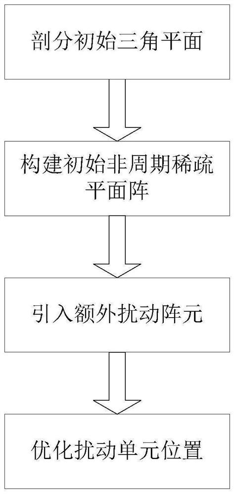
[0038] Such as figure 1 As shown, this embodiment provides a technical solution: a method for designing an aperiodic planar sparse phased array, including the following steps:

[0039] S1: Divide the initial triangular plane

[0040] Using three basic triangular surface elements, the initial triangular plane is completely subdivided;

[0041] S2: Construct the initial aperiodic sparse planar array

[0042] After subdivision, the vertices of all the basic triangular surface elements are used as the array element positions to form the initial aperiodic sparse planar array;

[0043] S3: Introducing additional perturbation elements

[0044] Introduce additional disturbance array elements at the same position inside each basic triangular surface element;

[0045] S4: Optimizing the position of the perturbation unit

[0046] Optimize the location of the perturbation element to improve the broadband low sidelobe index and scanning characteristics.

[0047] In the step S1, there...

Embodiment 2

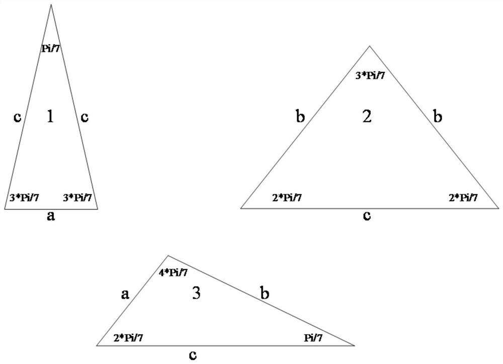
[0055] Such as figure 2 with 3 As shown, the three types of basic triangular surface elements (basic surface element 1, basic surface element 2, and basic surface element 3) can be filled to form a triangular plane similar to the surface element but with a larger size. Triangular planes with similar triangular facets can always be based on figure 2 According to the subdivision principle, it is divided into a series of 3 smaller basic surface elements.

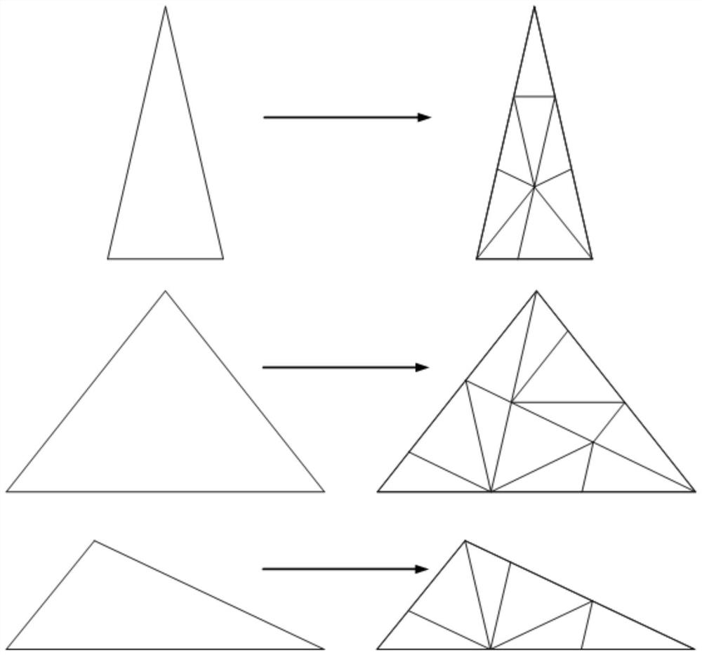
[0056] Such as Figure 4 As shown in , a schematic diagram of a triangle similar to the basic panel 2 undergoing three subdivision processes;

[0057] Such as Figure 5 As shown, for the array generation process in this embodiment, first in Figure 4 Array elements are arranged on the vertices of all basic triangular surface elements in the triangular plane three times, and 4 disturbance array elements are added inside each basic triangular surface element. The minimum distance between the array elements is 0.5 wavelengt...


PUM


Abstract

The invention discloses an aperiodic planar sparse phased array design method, which belongs to the technical field of array antenna design, and comprises the following steps: S1, subdividing an initial plane; s2, constructing an initial aperiodic sparse planar array; s3, introducing an extra disturbance array element; s4, optimizing positions of disturbance units. The three basic triangular surface elements are different in shape and size, and the initial triangular plane is similar to any one of the three basic triangular surface elements. The phased array designed by the invention has the excellent characteristics of wide frequency band, wide scanning angle and low sidelobe characteristic, and three different types of triangular planes are used as elements, so that an array with hundreds of array elements can be represented by using a small amount of variables, and the optimization process of a large-scale array is greatly simplified; besides, a CMA-ES optimization algorithm is adopted, and compared with a general genetic algorithm, a particle swarm optimization algorithm and the like, the method has better global search capability, so that the method is efficient, stable and worthy of popularization and application.

Description

technical field [0001] The invention relates to the technical field of array antenna design, in particular to a method for designing an aperiodic planar sparse phased array. Background technique [0002] Array antennas have high gain, beamforming, and space (beam) scanning characteristics, while phased array antennas are mainly used for phased array radars. For accurate tracking and identification of targets within the range, it is required to have low side lobes (high side lobes will introduce clutter and affect receiving efficiency), no grating lobes (grating lobes will occupy antenna radiation energy and affect antenna gain and efficiency), and broadband Band and low cost (fewer array elements) features. [0003] According to the antenna array theory, in order to suppress the side lobe, for the traditional periodic dense array, the array elements are required to be arranged periodically at the half-wavelength corresponding to the operating frequency, then because the "ha...

Claims


Application Information

Patent Timeline
Patent Type & Authority Applications(China)
IPC IPC(8): G06F30/20G06N3/00H01Q21/00
CPCG06F30/20G06N3/006H01Q21/00Y02D30/70
Inventor 王凯刘登宝李琳王蕾
Owner CHINA ELECTRONIC TECH GRP CORP NO 38 RES INST
Why Eureka
Try Eureka