High-speed high-precision time domain analog-to-digital converter
An analog-to-digital converter, time domain technology, applied in the direction of analog-to-digital converter, analog-to-digital conversion, code conversion, etc. Consumption controllable effect
- Summary
- Abstract
- Description
- Claims
- Application Information
AI Technical Summary
Problems solved by technology
Method used
Image
Examples
Embodiment 1
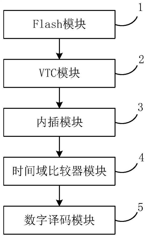
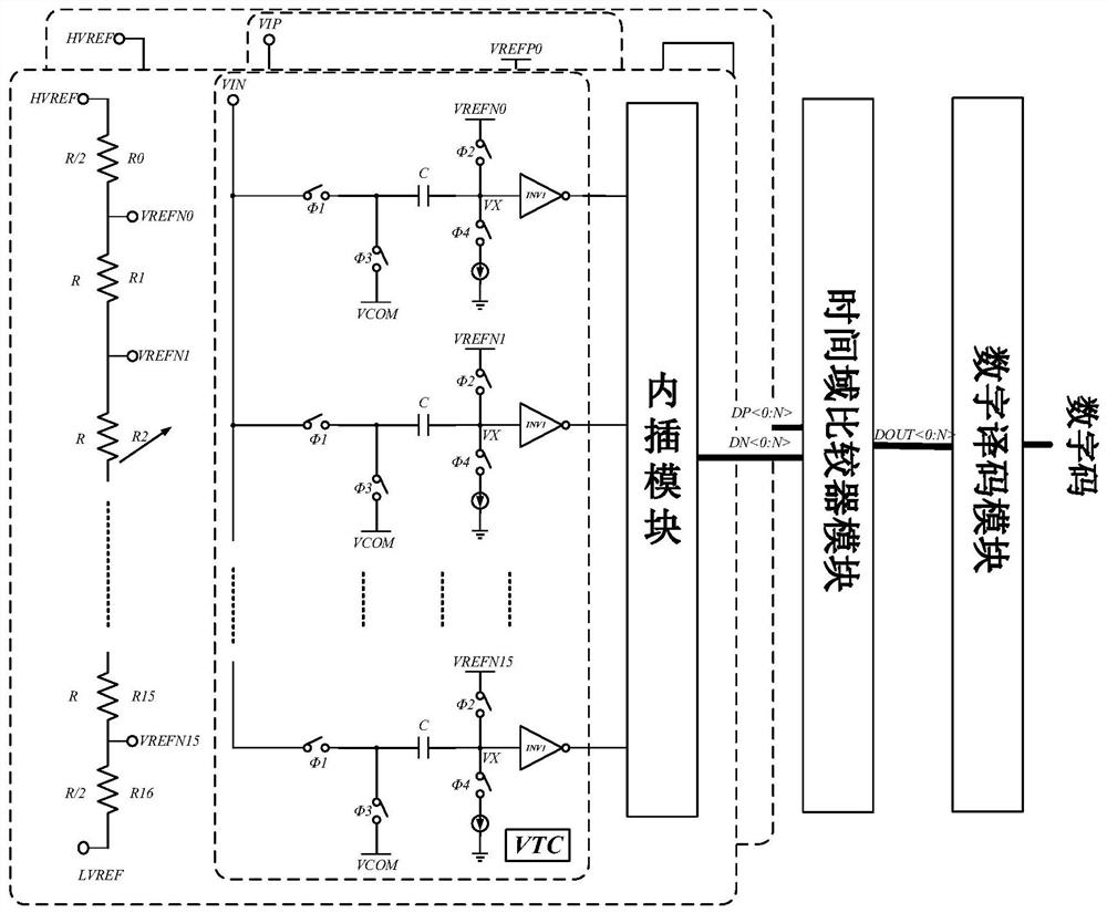
[0037] See figure 1 , figure 1 It is a schematic structural diagram of a high-speed and high-precision time-domain ADC provided by an embodiment of the present invention, including:
[0038] Flash module 1, used to generate a reference voltage;
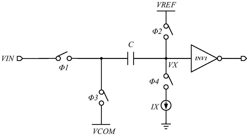
[0039] The VTC module 2 is connected to the Flash module 1, and is used to sample an input voltage signal and process the input voltage according to the reference voltage to obtain a first time signal;
[0040] An interpolation module 3, connected to the VTC module 2, for subdividing the first time signal to obtain a second time signal;
[0041] A time domain comparator module 4, connected to the interpolation module 3, for comparing the second time signal and outputting a thermometer code;
[0042] The digital decoding module 5 is connected to the time domain comparator module 4, and is used to convert the thermometer code into a binary code and output it.
[0043] Further, the Flash module 1 includes two Flash sub-modules, each ...
Embodiment 2
[0074] In order to further illustrate the effect of the present invention, in the above-mentioned embodiment one below figure 2 Provided time-domain ADC for simulation experiments. See Figure 7 , Figure 7 It is a VX node simulation waveform diagram provided by the embodiment of the present invention.
[0075] In this embodiment, for a clearer observation, only 6 outputs of the 16 outputs of the VTC whose slope signals are near the threshold voltage of the inverter are selected. Depend on Figure 7 The simulation waveform shows that during the Φ3 (or Φ4) phase period, except for vo4 and vo5, the other ramp signals will not cross the threshold voltage of the inverter in the Φ3 phase, and the corresponding inverter output is only to4 and to5 in the Φ3 phase. A level flip occurs. During the Φ3 phase, the signals above to4 are all low level, and the signals below to5 are all high level. So far, the VTC circuit has generated a 01 jump point and a time signal that are closel...
PUM
 Abstract
Description
Claims
Application Information
 - R&D
- Intellectual Property
- Life Sciences
- Materials
- Tech Scout
- Unparalleled Data Quality
- Higher Quality Content
- 60% Fewer Hallucinations
Browse by: Latest US Patents, China's latest patents, Technical Efficacy Thesaurus, Application Domain, Technology Topic, Popular Technical Reports.
© 2025 PatSnap. All rights reserved.Legal|Privacy policy|Modern Slavery Act Transparency Statement|Sitemap|About US| Contact US: help@patsnap.com


