

Organic compound and organic light-emitting device
An organic compound, selected technology, applied in the direction of organic chemistry, electrical solid-state devices, electrical components, etc., can solve the problems of low performance and not very good organic electroluminescent devices, achieve good life, improve exciton utilization, performance-enhancing effects
- Summary
- Abstract
- Description
- Claims
- Application Information
AI Technical Summary
Problems solved by technology
Method used
Image

Examples
Embodiment 1
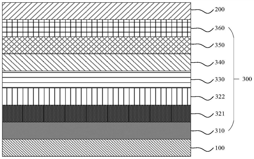
[0095] In a vacuum of 1×10 -5 Pa is deposited on a glass substrate with an anode of indium tin oxide (ITO) (thickness 100nm) by vacuum evaporation.
[0096] A compound HAT-CN was vapor-deposited on this substrate to form a hole injection layer (HIL) with a film thickness of 60 nm.
[0097] On the hole injection layer (HIL), compound NPB was then vapor-deposited to form a hole transport layer (HTL) with a thickness of 20 nm.
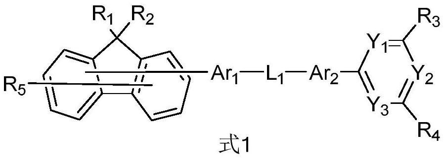
[0098] Compound 1 and Compound 2 were co-evaporated on the hole transport layer (HTL) to form an emitting layer (EML) with a thickness of 35 nm. The concentration of Compound 2 in the light-emitting layer (EML) was 97%, and the concentration of Compound B was 3%.
[0099] Compound A-2 and LiQ were co-evaporated on the emitting layer (EML), and the two materials were vaporized at the same rate to form an electron transport layer (ETL) with a thickness of 35 nm.
[0100] LiF was vapor-deposited on the electron transport layer (ETL) to form an electron in...
Embodiment 2-3
[0105] Using the compounds in Table 1 instead of Compound A-2, the same method as in Example 1 was used to fabricate an organic light-emitting device.
PUM
| Property | Measurement | Unit |
|---|---|---|
| Thickness | aaaaa | aaaaa |
Abstract
Description
Claims
Application Information