Silicon waveguide end face coupling structure and manufacturing method thereof

A technology of end-face coupling and silicon waveguide, which is applied in the field of silicon waveguide end-face coupling structure and its manufacture, can solve the problems of large coupling loss of ordinary single-mode optical fiber and small size of silicon waveguide mode field, and achieve low-loss coupling and simple preparation process Effect

Active Publication Date: 2020-09-18
TSINGHUA UNIV
View PDF7 Cites 9 Cited by
  • Summary
  • Abstract
  • Description
  • Claims
  • Application Information

AI Technical Summary

Problems solved by technology

[0006] The purpose of the embodiments of the present invention is to provide a silicon waveguide end-face coupling structure and its manufacturing method to solve the technical problems of the silicon waveguide mode field size being small and the ordinary single-mode fiber coupling loss existing in the prior art

Method used


Image

  • Silicon waveguide end face coupling structure and manufacturing method thereof
  • Silicon waveguide end face coupling structure and manufacturing method thereof
  • Silicon waveguide end face coupling structure and manufacturing method thereof

Examples


Embodiment Construction

[0029] The specific implementation manners of the present invention will be further described in detail below in conjunction with the accompanying drawings and embodiments. The following examples are used to illustrate the present invention, but are not intended to limit the scope of the present invention.

[0030] In the description of the present invention, it should be noted that unless otherwise specified and limited, the terms "installation", "connection" and "connection" should be understood in a broad sense, for example, it can be a fixed connection or a detachable connection. Connected, or integrally connected; it may be mechanically connected or electrically connected; it may be directly connected or indirectly connected through an intermediary, and it may be the internal communication of two components. Those of ordinary skill in the art can understand the specific meanings of the above terms in the present invention in specific situations.

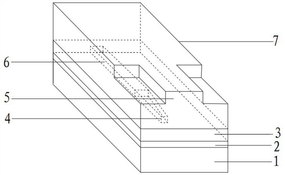
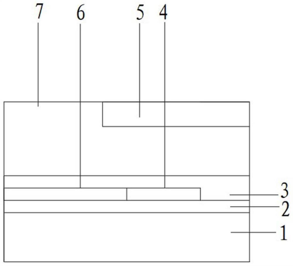
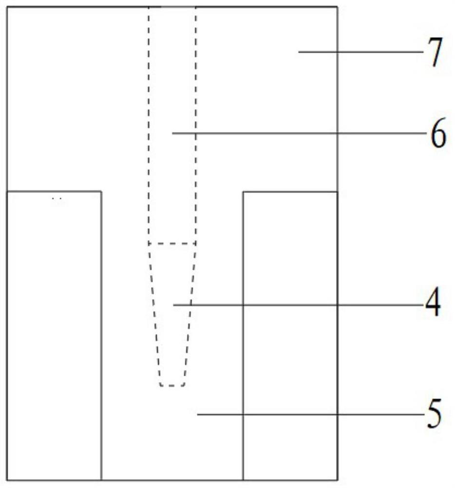
[0031] Such as Figure...


PUM

PropertyMeasurementUnit
heightaaaaaaaaaa
widthaaaaaaaaaa
lengthaaaaaaaaaa

Abstract

The invention relates to the technical field of photonic integrated devices, and discloses a silicon waveguide end face coupling structure and a manufacturing method thereof. The structure comprises substrate silicon, an oxide layer, a silicon waveguide and a silicon nitride layer which are sequentially stacked from bottom to top, the end of the silicon nitride layer is of a ridge-shaped structureto form a ridge-shaped silicon nitride waveguide, and the ridge-shaped silicon nitride waveguide is used for being coupled with the end face of a common single-mode optical fiber. The method comprises the following steps of preparing a silicon waveguide by using a thin film silicon layer positioned on an oxide layer on the upper surface of substrate silicon in a silicon-on-insulator substrate, preparing a pointed cone structure of which the width is gradually reduced at one end, coupled with the optical fiber, of the silicon waveguide to form a silicon waveguide pointed cone structure, depositing a silicon nitride layer on the silicon waveguide and the oxide layer, and carrying out shallow etching on the silicon nitride layer to prepare a ridge-shaped structure so as to form the ridge-shaped silicon nitride waveguide. The ridge-shaped silicon nitride waveguide conversion mode field can be matched with a common single-mode optical fiber, and is suitable for low-loss coupling of the silicon waveguide and the common single-mode optical fiber in the silicon photonic chip packaging process.

Description

technical field [0001] The invention relates to the technical field of photonic integrated devices, in particular to a silicon waveguide end face coupling structure and a manufacturing method thereof. Background technique [0002] Silicon photonic integration based on silicon waveguides has become a key technology for the development of high-performance and low-cost optical communication components and photonic integrated devices. This silicon photonic chip is generally prepared on a silicon on insulator (silicon on insulator, SOI for short) substrate, using silicon material as the core part of the waveguide, and the cross-sectional size of the core area is on the order of hundreds of nanometers. The waveguide cladding material generally adopts silicon dioxide. Due to the high refractive index contrast between crystalline silicon and silicon dioxide, the silicon waveguide mode field area is generally less than 1 square micron, so it can support high-density photonic integra...

Claims


Application Information

Patent Timeline
Patent Type & Authority Applications(China)
IPC IPC(8): G02B6/122G02B6/136G02B6/13
CPCG02B6/1228G02B6/13G02B6/136G02B2006/12097G02B2006/12176
Inventor 张巍顿鹏翔黄翊东冯雪刘仿崔开宇
Owner TSINGHUA UNIV
Why Eureka
Try Eureka