
Method for improving total dose irradiation resistance of FinFET device

A technology with anti-total dose and radiation performance, applied in the fields of semiconductor devices, electric solid-state devices, semiconductor/solid-state device components, etc., can solve the problems of threshold voltage drift, increase of off-state leakage current, etc., to reduce the impact and cost. The effect of improving and improving the anti-total dose radiation performance

Inactive Publication Date: 2020-09-22
PEKING UNIV
View PDF7 Cites 0 Cited by
  • Summary
  • Abstract
  • Description
  • Claims
  • Application Information

AI Technical Summary

Problems solved by technology

Existing studies have shown that FinFET devices undergo degradation phenomena such as increased off-state leakage current and threshold voltage drift after being irradiated by the total dose.

Method used


Image

  • Method for improving total dose irradiation resistance of FinFET device
  • Method for improving total dose irradiation resistance of FinFET device

Examples


Embodiment 1

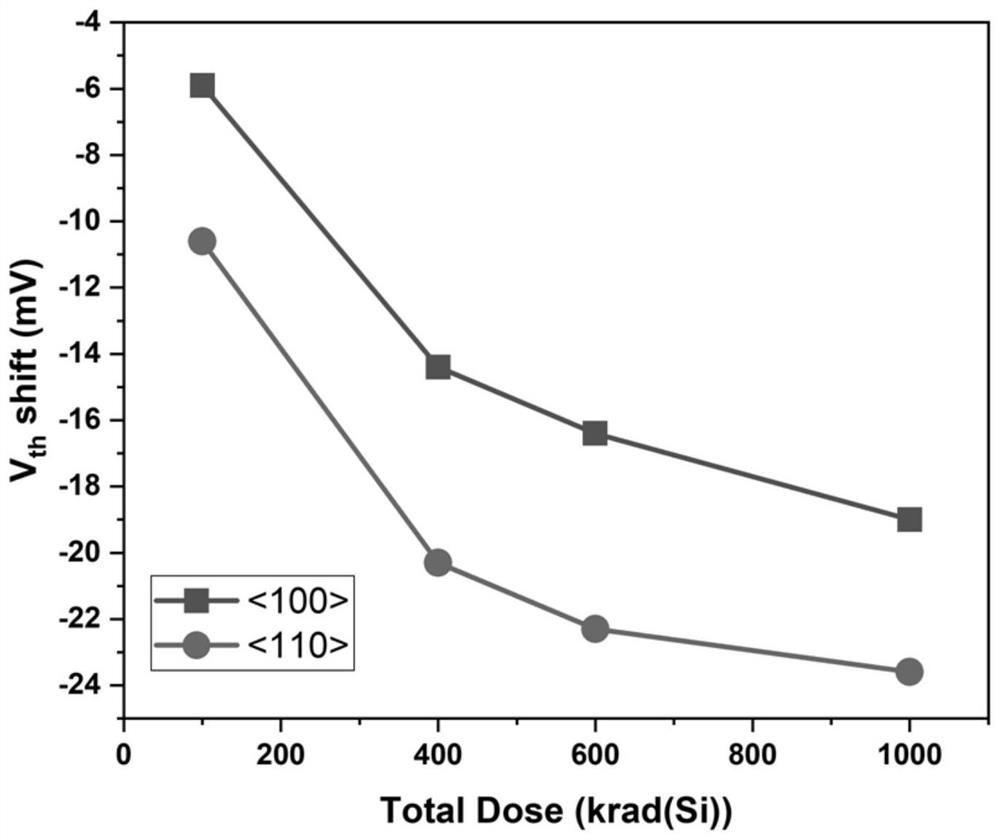
[0016] Example 1: P-type FinFET devices with channel orientations of and were prepared on the same bulk silicon (100) wafer, and their anti-total dose radiation performance was compared. Specific steps are as follows:

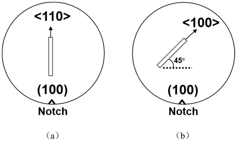
[0017] Step 1. Design P-type FinFET device layouts with channel crystal orientations of and on a (100) bulk silicon wafer. Except for different channel crystal orientations, other parameters are the same. For (100) wafers, the positioning mark (Notch) is downward as the positive direction, and the crystal orientation in the horizontal axis direction is . Ordinary layout FinFET device channel crystal orientation is , such as figure 1 It is shown in the middle left figure (a). The direction forming an angle of 45° with the horizontal axis is the channel direction of the FinFET device proposed by the present invention, and the crystal direction of the FinFET channel is , such as figure 1 As shown in the middle right figure (b);

[0018] Step 2. Prepare two...


PUM


Abstract

The invention discloses a method for improving the total dose irradiation resistance of a FinFET device. According to the method, the trap charge density of an oxide layer and the crystal orientationdependence of an interface state are utilized; during layout design, the placement direction of the device is properly adjusted; the channel crystal orientation of the FinFET device is ensured to be (100), so the oxide layer trapped charge density and the interface state density generated in the prepared FinFET device by the total dose irradiation are lower, the influence of the total dose irradiation on the FinFET device is reduced, and the total dose irradiation resistance of the FinFET device is improved.

Description

technical field [0001] The invention relates to a method for improving the anti-total dose radiation performance of a Fin Field Effect Transistor (FinFET), which belongs to the technical field of VLSI manufacturing. Background technique [0002] With the rapid development of integrated circuit technology, the feature size of devices has been reduced to the nanometer scale. FinFET devices have good gate control capabilities and can overcome the problems of short channel effects and mobility degradation faced by traditional planar bulk silicon devices. Starting from the 22nm technology node, FinFET has become the mainstream device in the manufacture of nanoscale VLSI. Depending on the substrate, FinFET devices can be classified into bulk silicon FinFET devices and silicon-on-insulator (SOI) FinFET devices. On the other hand, with the rapid development of aerospace technology, more and more integrated circuits work in the space radiation environment. After microelectronic de...

Claims


Application Information

Patent Timeline
Patent Type & Authority Applications(China)
IPC IPC(8): H01L29/04H01L29/78H01L23/552
CPCH01L23/552H01L29/045H01L29/785
Inventor 安霞任哲玄李艮松陈珙黎明黄如张兴
Owner PEKING UNIV
Learn More