A two-dimensional material transfer method based on a stepped substrate

A technology of two-dimensional materials and transfer methods, which is applied in the field of material transfer, can solve the problems of the contact area between two-dimensional materials and the substrate becomes smaller and cannot be transferred, and achieve the effects of increasing the bonding force, improving the success rate, and reducing costs

Active Publication Date: 2022-06-28
SOUTHEAST UNIV
View PDF16 Cites 0 Cited by
  • Summary
  • Abstract
  • Description
  • Claims
  • Application Information

AI Technical Summary

Problems solved by technology

When there are electrodes (or other steps) on the surface of the target substrate that cause the substrate to be uneven, these traditional methods will not be able to transfer to the designated position due to the smaller contact area between the two-dimensional material and the substrate

Method used


Image

  • A two-dimensional material transfer method based on a stepped substrate
  • A two-dimensional material transfer method based on a stepped substrate

Examples


Embodiment 1

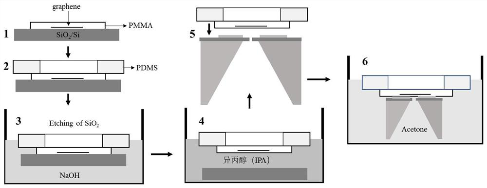
[0020] like figure 1 The two-dimensional material transfer method based on the stepped substrate shown includes the preparation and transfer process of the two-dimensional material. The preparation of the two-dimensional material adopts the mechanical lift-off method, and the transfer adopts the improved wet transfer method. In this example, the two-dimensional material is to be transferred. The material is graphene.

[0021] Specifically include the following steps:

[0022] (1) Graphene is peeled off on a silicon oxide / silicon substrate to form a graphene layer, preferably a silicon oxide / silicon substrate with a thickness of 285 nanometers of silicon oxide, and spin-coating 4% PMMA benzene on the graphene layer Diethyl ether solution, spin-coated 2 times to ensure the thickness of the PMMA film is 0.5 μm.

[0023] Graphene can also be exfoliated on PMMA first and then pressed onto a silicon oxide / silicon substrate.

[0024] (2) Under the optical microscope, the graphene / ...

Embodiment 2

[0034] The present invention is based on a two-dimensional material transfer method with a stepped substrate, which specifically includes the following steps:

[0035] (1) peel off the graphene on the silicon oxide / silicon substrate to form a graphene layer, spin-coat PMMA on the graphene layer, and spin-coat twice to ensure that the thickness of the PMMA film is 0.65 microns;

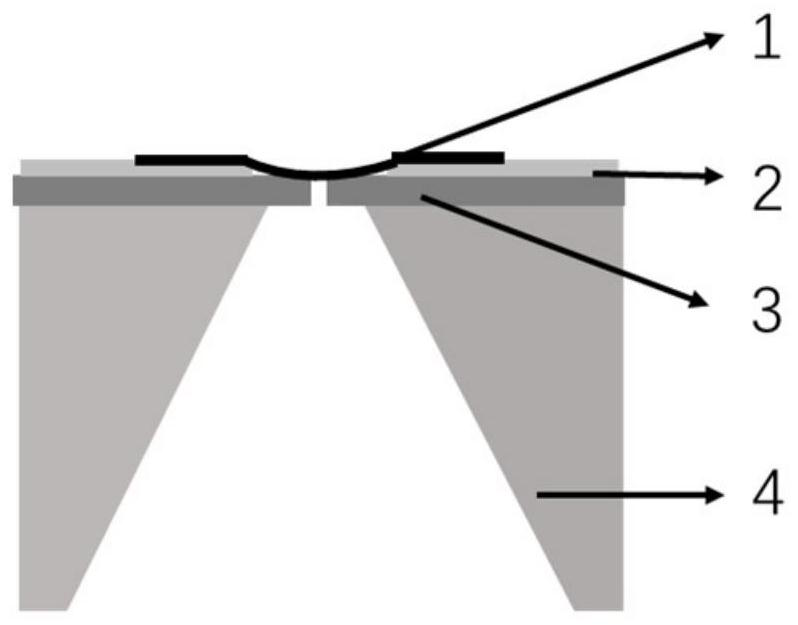
[0036] (2) Under the optical microscope, the graphene / PMMA layer was pressed tightly onto the punched PDMS square, and the graphene was located in the center of the hole; a cylindrical puncher was used, and the hole diameter was 2.5 mm.

[0037] (3) Put the whole sample obtained into sodium hydroxide solution to etch silicon oxide to release graphene / PMMA / PDMS; the mass fraction of sodium hydroxide solution is 33%.

[0038] (4) fish out the graphene / PMMA / PDMS and put it into isopropanol solution for cleaning, then fish out the graphene / PMMA / PDMS, align the graphene with the target position and press it...

Embodiment 3

[0041] The present invention is based on a two-dimensional material transfer method with a stepped substrate, which specifically includes the following steps:

[0042] (1) peel off the graphene on the silicon oxide / silicon substrate to form a graphene layer, spin-coat PMMA on the graphene layer, and spin-coat 3 times to ensure that the thickness of the PMMA film is 0.8 microns;

[0043] (2) Under an optical microscope, the graphene / PMMA layer was pressed onto the punched PDMS square, and the graphene was located in the center of the hole; a cylindrical puncher was used, and the hole diameter was 3 mm.

[0044] (3) Putting the obtained whole sample into sodium hydroxide solution to etch silicon oxide to release graphene / PMMA / PDMS; the mass fraction of sodium hydroxide solution is 35%.

[0045] (4) fish out the graphene / PMMA / PDMS and put it into isopropanol solution for cleaning, then fish out the graphene / PMMA / PDMS, align the graphene with the target position and press it with ...


PUM

PropertyMeasurementUnit
thicknessaaaaaaaaaa
thicknessaaaaaaaaaa

Abstract

The invention discloses a two-dimensional material transfer method based on a stepped substrate, comprising the following steps: making a two-dimensional material layer on the substrate, spin-coating PMMA, making PDMS / PMMA / two-dimensional material / substrate, etching the lining The silicon oxide on the bottom releases the PDMS / PMMA / two-dimensional material, combines the two-dimensional material to be transferred with the target substrate, and dissolves PMMA. This transfer method is suitable for flat substrates and substrates with steps caused by electrode addition; at the same time, the method of direct wet etching with sodium hydroxide solution ensures that two-dimensional materials, especially graphene, can be transferred during the transfer process. There will be no curling, which improves the success rate of transfer and reduces costs; use isopropanol instead of deionized water to clean the 2D material after etching silicon oxide, one is because isopropanol is volatile, and the other is because in two-dimensional When the material is combined with the target substrate and PMMA is etched, isopropanol can increase the bonding force between the two-dimensional material and the substrate, and will not cause the two-dimensional material to curl and shift.

Description

technical field [0001] The invention relates to the technical field of material transfer, in particular to a two-dimensional material transfer method based on a stepped substrate. Background technique [0002] Currently commonly used two-dimensional materials include graphene, molybdenum disulfide, tungsten disulfide and boron nitride, etc. Since graphene was first discovered in 2004, the research and application of two-dimensional materials has developed rapidly, in the fields of biological detection and microelectronics. There are broad application prospects. At present, the main methods for preparing two-dimensional materials include mechanical exfoliation method, chemical redox method and vapor deposition method. Among them, mechanical exfoliation method is the main method for preparing two-dimensional material samples in general experimental research. The quality of 2D materials with thin layers is higher. Regardless of the fabrication method, the next step is to tran...

Claims


Application Information

Patent Timeline
Patent Type & Authority Patents(China)
IPC IPC(8): C01B32/194C01B21/064C01G39/06
CPCC01B32/194C01B21/0648C01G39/06
Inventor 毕可东郭明齐晗
Owner SOUTHEAST UNIV
Why Eureka
Try Eureka