Low-voltage ESD protection device and manufacturing method thereof

A technology of ESD protection and manufacturing method, which is applied in the field of electronic science and technology, can solve the problems of high ESD trigger voltage, low current density, high ESD, etc., and achieve the effect of reducing chip area occupation, reducing chip cost, and optimizing device size

Pending Publication Date: 2020-09-25
江苏吉莱微电子股份有限公司 +1
View PDF0 Cites 2 Cited by
  • Summary
  • Abstract
  • Description
  • Claims
  • Application Information

AI Technical Summary

Problems solved by technology

[0004] The purpose of the present invention is to provide a low-voltage ESD protection device and a manufacturing method thereof. For specific low-voltage applications of 1V to 3.3V, it is dedicated to obtaining an ESD protection device with a low trigger voltage and a high ESD discharge current in the true sense, and solves the current problem. Issues such as high ESD trigger voltage and low 8 / 20 current density used in the low-voltage system at the stage

Method used


Image

  • Low-voltage ESD protection device and manufacturing method thereof
  • Low-voltage ESD protection device and manufacturing method thereof
  • Low-voltage ESD protection device and manufacturing method thereof

Examples


Embodiment Construction

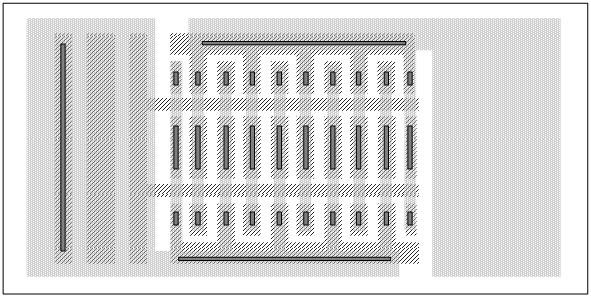
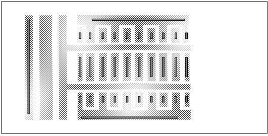
[0037] Such as Figure 1-15 As shown, a low-voltage ESD protection device includes an N-type single crystal material layer 101, an N+ polysilicon 103, an N-type base region 104, and a P-type base region 105. The N-type single crystal material layer 101 is provided with a first layer of isolation medium 108. The first metal layer 109, the second layer of isolation dielectric 110, the second metal layer 111, the N+ polysilicon 103, the N-type base region 104, and the P-type base region 104 are all set on the top of the N-type single crystal material layer 101, and the N+ polysilicon 103 is provided with a P+ source region 106 and an N+ source region 107, a thermal oxide layer 102 is provided between the outside and the N-type single crystal material layer 101, and a P+ source region 106 and a P-type base region 105 are provided in the N-type base region 104. A P+ source region 106 , an N+ source region 107 , an N+ source region 107 , and a P+ source region 106 are sequentially a...


PUM

PropertyMeasurementUnit
electrical resistivityaaaaaaaaaa
thicknessaaaaaaaaaa

Abstract

The invention discloses a low-voltage ESD protection device and a manufacturing method thereof, which effectively improve the utilization rate of a chip and reduce the cost of the chip. The cell sizeis not increased, the chip area occupation caused by keeping the metal spacing is reduced, the cell size can be reduced by about 20%, and the current discharge capacity is at least improved by 50%; flyback current of the SCR can be reduced to 1.5 V by adopting a forward bias diode string, and ultralow trigger voltage ESD protection devices with voltage classes of 1.2V, 1.8V, 2V, 2.5V, 2.8V, 3.3V and the like can be realized by adjusting the number of forward bias diodes; by optimizing the device size and the ultralow residual voltage, the device is suitable for ultra-high-speed signal protection of a low-voltage system, meanwhile, bidirectional ESD protection can be achieved through layout optimization, and a solution is provided for bidirectional protection of ultra-high-speed signals ofthe low-voltage system.

Description

technical field [0001] The invention relates to the field of electronic science and technology, in particular to a low-voltage ESD protection device and a manufacturing method thereof. Background technique [0002] Nowadays, the era of artificial intelligence combined with the Internet of Things is officially coming, and smart homes are also playing an increasingly important role in life. With the continuous development of technology, the chips required by the Internet of Things are further developed towards high integration and lower power consumption, which also requires the line width of its manufacturing process to be further reduced. The narrow line width and low power consumption also make the chip more fragile and sensitive when it is subjected to electrostatic discharge effects, resulting in more and more stringent electrostatic discharge tests. With the further reduction of power consumption, the power supply voltage is also further reduced, and there are further r...

Claims


Application Information

Patent Timeline
Patent Type & Authority Applications(China)
IPC IPC(8): H01L27/02H01L27/06H01L21/8222
CPCH01L21/8222H01L27/0262H01L27/0647
Inventor 杨珏琳宋文龙李泽宏张鹏
Owner 江苏吉莱微电子股份有限公司
Why Eureka
Try Eureka