Gating tube material, gating tube unit and manufacturing method thereof
A technology of gate tube and material layer, applied in the field of micro-nano electronics, can solve the problem of large turn-on voltage, and achieve the effects of small turn-on voltage, high driving force, and low leakage conductance
- Summary
- Abstract
- Description
- Claims
- Application Information
AI Technical Summary
Problems solved by technology
Method used
Image

Examples
Embodiment 1
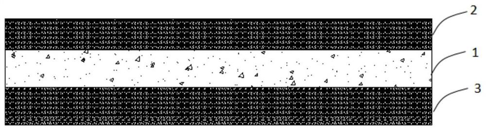
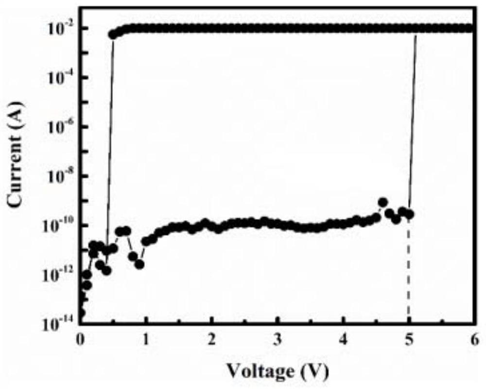
[0053] Such as figure 2 as shown, figure 2 The voltage-current curve of the gating tube unit that is the germanium sulfide (GeS) material preparation in the prior art; The gating tube material layer 1 that the thickness that uses material germanium sulfide (GeS) to obtain is 20 nanometers, and the second electrode 3 is the diameter The first electrode 2 is an aluminum electrode, and a 10 nanometer thick titanium nitride (TiN) transition layer is provided between the first electrode 2 and the material layer 1 of the gate tube.
[0054] Such as figure 2 As shown, when the voltage applied to the gate unit is less than 5V, the gate unit is in the off state, and the leakage current is less than 10 -10 A; When the voltage applied to the gate unit exceeds the threshold voltage, the gate unit is instantly opened, and the current through the gate unit increases sharply to 10 -2 A: When the voltage applied to the gating tube unit is removed (that is, the voltage is 0.5V), the gati...
Embodiment 2
[0063] The through tube material provided by this application combines the GeS target with the As 2 Te 3 The target is obtained by co-sputtering and co-sputtering;
[0064] The gating tube unit disclosed in this application includes a first electrode layer 2, a second electrode layer 3 and a gating tube material layer 1, wherein the gating tube material layer 1 is obtained by sputtering the above gating tube material, and the first electrode 2 is located on the upper surface of the gate material layer 1; the second electrode 3 is located on the lower surface of the gate material layer 1;
[0065] The material of the first electrode layer 2 is aluminum with a thickness of 190 nanometers, the material of the second electrode layer 3 is aluminum with a thickness of 190 nanometers, and the thickness of the gate tube material layer 1 is 20 nanometers.
[0066] Moreover, a transition layer is provided on the upper surface of the gate material layer 1, and the first electrode 2 is ...
PUM
| Property | Measurement | Unit |
|---|---|---|
| thickness | aaaaa | aaaaa |
| thickness | aaaaa | aaaaa |
| thickness | aaaaa | aaaaa |
Abstract
Description
Claims
Application Information
 - R&D
- Intellectual Property
- Life Sciences
- Materials
- Tech Scout
- Unparalleled Data Quality
- Higher Quality Content
- 60% Fewer Hallucinations
Browse by: Latest US Patents, China's latest patents, Technical Efficacy Thesaurus, Application Domain, Technology Topic, Popular Technical Reports.
© 2025 PatSnap. All rights reserved.Legal|Privacy policy|Modern Slavery Act Transparency Statement|Sitemap|About US| Contact US: help@patsnap.com