A kind of asymmetric structure high-power laser with Bragg reflector and its preparation method
A high-power laser and Bragg reflector technology, applied in the field of lasers, can solve the problems of sensitive working temperature, large diffusion coefficient, sensitive memory effect, etc., and achieve the effects of wide wavelength tuning range, high power stability, and narrow spectral line width.
- Summary
- Abstract
- Description
- Claims
- Application Information
AI Technical Summary
Problems solved by technology
Method used
Image
Examples
Embodiment 1
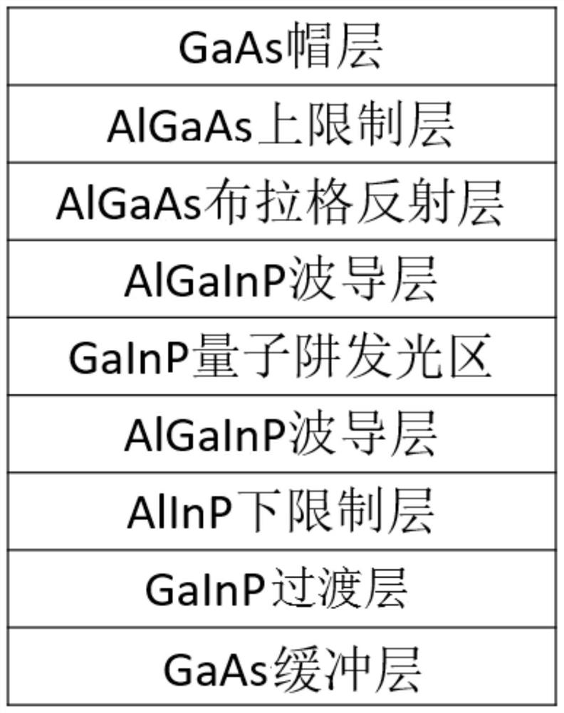
[0056] An asymmetric high-power laser with a Bragg reflector, such as figure 1 As shown, the GaAs substrate is included, and the GaAs buffer layer, GaAs buffer layer, Ga 1-x In x P transition layer, Al 1-x In x P lower confinement layer, (Al 1-x Ga x ) y In 1-y P lower waveguide layer, Ga 1-x In x P quantum well light-emitting region, (Al 1-x Ga x ) y In 1-y P upper waveguide layer, Al 1-x Ga x As Bragg reflector, Al 1-x Ga x As upper confinement layer and GaAs cap layer.
Embodiment 2
[0058] A kind of asymmetric structure high-power laser with Bragg reflector, structure as shown in embodiment 1, difference is, (Al 1-x Ga x ) y In 1-y The thickness of the waveguide layer under P is related to (Al 1-x Ga x ) y In 1-y The waveguide layers on P have different thicknesses, preferably 0.12 μm and 0.07 μm respectively.
Embodiment 3
[0060] A preparation method of an asymmetric structure high-power laser with a Bragg reflector, comprising the steps of:
[0061] (1) Put GaAs substrate in MOCVD equipment, H 2 The environment is heated to 720±10°C and baked for 30 minutes, and AsH is introduced 3 , remove water and oxygen on the surface of the GaAs substrate to complete the surface heat treatment, and prepare for step (2);
[0062] (2) Slowly lower the temperature to 700±10°C, and continue to feed TMGa and AsH 3 , grow a GaAs buffer layer with a thickness of 0.3 μm on the GaAs substrate;
[0063] (3) Keep the temperature at 700±10°C, continue to feed TMIn, TMGa and PH 3 , grow Ga on the GaAs buffer layer in step (2) 1-x In x P transition layer;
[0064] (4) Keep the temperature at 700±10°C, continue to feed TMIn, TMAl and PH 3 , Ga in step (3) 1-x In x Growth of n-type Al on P transition layer 1-x In x P lower limit layer;
[0065] (5) The temperature is lowered to 650±10°C, and TMIn, TMAl, TMGa a...
PUM
| Property | Measurement | Unit |
|---|---|---|
| thickness | aaaaa | aaaaa |
| thickness | aaaaa | aaaaa |
| thickness | aaaaa | aaaaa |
Abstract
Description
Claims
Application Information
