Preparation method of ridge-type GaAs-based laser with asymmetric injection window

A laser, asymmetric technology, applied in the structure of the active area, the structure of the optical waveguide semiconductor, etc., can solve the problem of ignoring the control of the divergence angle, and achieve the effect of suppressing optical catastrophe damage, reducing the spot pattern, and improving the COD threshold.

Active Publication Date: 2020-10-09
潍坊华光光电子有限公司
View PDF29 Cites 1 Cited by
  • Summary
  • Abstract
  • Description
  • Claims
  • Application Information

AI Technical Summary

Problems solved by technology

The aforementioned technologies have adopted a series of measures to increase the initial bandgap of the cavity surface area to improve the laser’s ability to resist COD, but neglected the control of the divergence angle. After the anti-COD ability increases, the divergence angle will change, and the divergence angle will affect the later use of the laser. effect plays a more important role

Method used


Image

  • Preparation method of ridge-type GaAs-based laser with asymmetric injection window
  • Preparation method of ridge-type GaAs-based laser with asymmetric injection window
  • Preparation method of ridge-type GaAs-based laser with asymmetric injection window

Examples


Embodiment 1

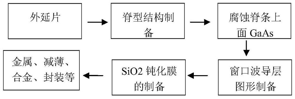
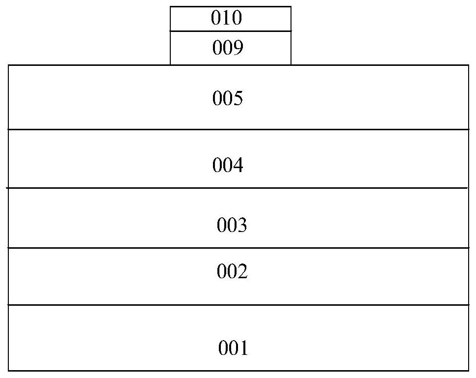
[0031] A method for preparing a ridge GaAs-based laser with an asymmetric injection window. The laser includes an epitaxial wafer. The epitaxial wafer includes a substrate, an N confinement layer, a lower waveguide layer, a quantum well active region, and an upper waveguide arranged in sequence from bottom to top Layer, P confinement layer and ohmic contact layer, the preparation methods are as follows figure 1 As shown, the steps are as follows:

[0032] Step (1). A ridge structure is etched on the upper surface of the epitaxial wafer. The ridge structure is located at the center of the epitaxial wafer. The areas other than the ridge structure are etched to the upper waveguide layer, and the ridge structure remains To the ohmic contact layer, the ridge structure runs through the entire cavity length of the epitaxial wafer; figure 2 Shown.

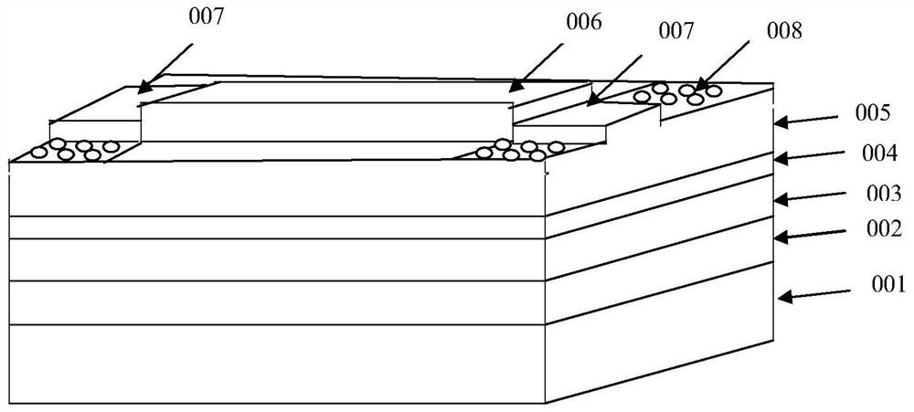
[0033] Step (2): Divide the ridge structure into a ridge light-emitting area and a window area. The window areas are located at both ends of ...

Embodiment 2

[0040] A method for preparing a ridge GaAs-based laser with an asymmetric injection window. The steps are the same as those described in Embodiment 1, except that in step (1), the ridge structure is located on one side of the epitaxial wafer.

Embodiment 3

[0042] A method for preparing a ridge GaAs-based laser with an asymmetric injection window. The steps are the same as those described in Embodiment 1, except that in step (3), the prepared pattern is elliptical.


PUM


Abstract

The invention relates to a preparation method of a ridge-type GaAs-based laser with an asymmetric injection window, and belongs to the technical field of semiconductor laser preparation. The method comprises the following steps: corroding a ridge-shaped structure on the surface of an epitaxial wafer; completely corroding the P limiting layer and the ohmic contact layer outside the ridge-shaped structure; etching off the ohmic contact layer on the ridge-shaped structure of the window region; corroding four sides of the window area except the ridge-shaped structure to the area of the waveguide layer; preparing a pattern in a regular shape through photoetching, corrosion and other methods, then preparing a current injection window in a ridge-shaped light-emitting area through PECVD and photoetching processes, and finally enabling a prepared sample to be subjected to the working steps of electrode deposition, thinning, alloying, packaging and the like to form the laser. The divergence angle of the light spot pattern is changed through the change of the refractive index of the waveguide layer, the absorption of light near the cavity surface is limited, the COD threshold of the high-power semiconductor laser is effectively improved, the divergence angle is restrained, and the light spot quality is improved.

Description

Technical field [0001] The invention relates to a method for preparing a ridge GaAs-based laser with an asymmetric injection window, and belongs to the technical field of semiconductor lasers. Background technique [0002] Since the advent of semiconductor lasers, due to its small size, high power, long life, and easy use, it has been favored in various fields. High-power semiconductor lasers have the advantages of small size, light weight, high efficiency, wide range of coverage, easy integration, etc., are widely used, and higher requirements are put forward for their output power and beam quality performance. In the process of increasing the output power of high-power semiconductor lasers, the appearance of cavity surface optical catastrophic damage (COD) has become one of the main limiting factors. Cavity surface optical catastrophic damage (COD) Because the laser cavity surface is located at the edge of the heat sink, the heat dissipation is poor. The electron-hole pairs ge...

Claims


Application Information

Patent Timeline
Patent Type & Authority Applications(China)
IPC IPC(8): H01S5/22H01S5/34
CPCH01S5/22H01S5/34
Inventor 陈康王金翠苏建任夫洋殷方军
Owner 潍坊华光光电子有限公司
Why Eureka
Try Eureka