Thinned wafer packaging process using TSV and TGV
A wafer packaging and wafer technology, applied in the manufacture of electrical components, electrical solid devices, semiconductor/solid devices, etc., can solve problems such as uneven stress, fragmentation or mechanical damage
- Summary
- Abstract
- Description
- Claims
- Application Information
AI Technical Summary
Problems solved by technology
Method used
Image

Examples
Embodiment 1
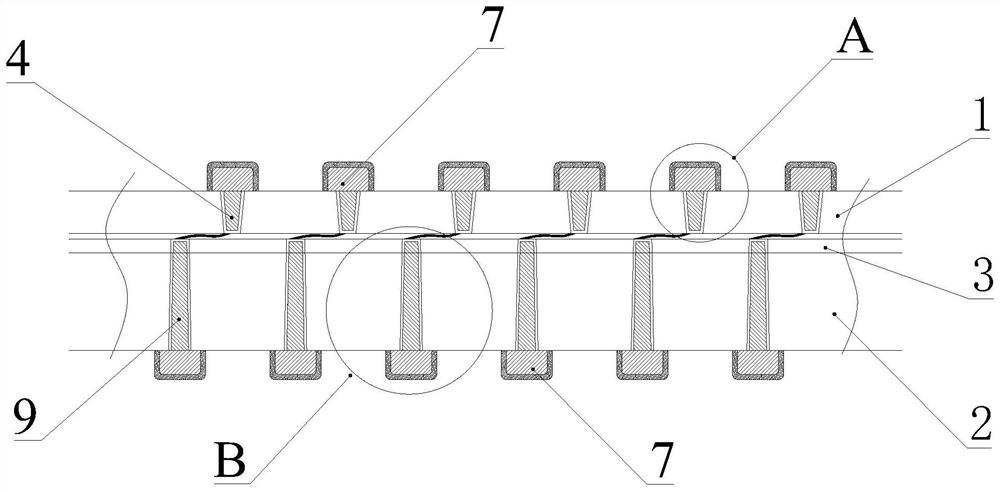
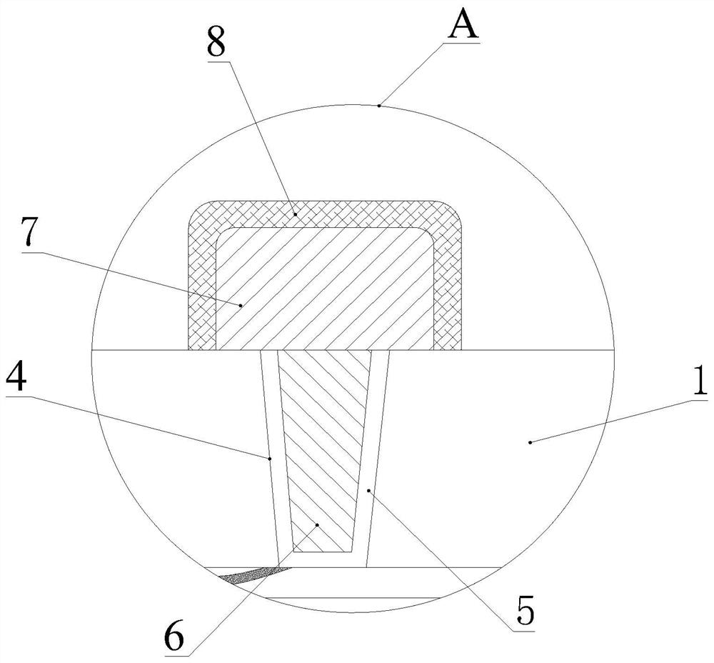
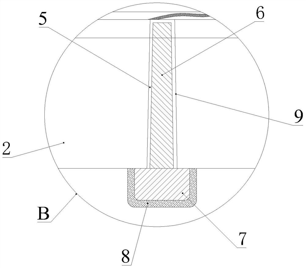
[0046] A thinning wafer packaging process utilizing TSVs, comprising the following steps:
[0047] S1. Perform RDL wiring on the front of the wafer through the yellow light process, and then bond the front of the wafer to a glass carrier to complete the thinning of the back side, and make TSV vias on the back of the wafer through the yellow light process or Laser perforation combined with etching technology;
[0048] S2. Electroless plating of a Ni / Pd / Cu seed layer on the side wall and bottom of the TSV via hole;
[0049] S3, then fill Cu into the TSV via hole by electroplating, and polish the back of the wafer by chemical mechanical planarization CMP to complete the filling of the TSV via hole;
[0050]S4. Coating photoresist on the back of the wafer, and making Cu Pillar on the back of the wafer corresponding to the TSV via hole through the ECP process;
[0051] S5. Electroless plating is performed on the Cu Pillar surface of the copper pillar bump of the wafer to form a Ni...
Embodiment 2
[0056] A thinning wafer packaging process utilizing TSVs and TGVs, comprising the following steps:
[0057] S1. Perform RDL wiring on the front of the wafer through the yellow light process, and then bond the front of the wafer to a glass carrier to complete the thinning of the back side, and make TSV vias on the back of the wafer through the yellow light process or Laser perforation combined with etching technology;
[0058] S2. Electroless plating of a Ni / Pd / Cu seed layer on the side wall and bottom of the TSV via hole;
[0059] S3, then fill Cu into the TSV via hole by electroplating, and polish the back of the wafer by chemical mechanical planarization CMP to complete the filling of the TSV via hole;
[0060] S4. Coating photoresist on the back of the wafer, and making Cu Pillar on the back of the wafer corresponding to the TSV via hole through the ECP process;
[0061] S5. Electroless plating is performed on the Cu Pillar surface of the copper pillar bump of the wafer to...
PUM
 Abstract
Description
Claims
Application Information