

Digital control variable gain amplifier
A gain amplifier, digital control technology, applied in gain control, amplification control, electrical components, etc., can solve problems such as mismatch, difficulty in achieving gain control gain step size, etc.
- Summary
- Abstract
- Description
- Claims
- Application Information
AI Technical Summary
Problems solved by technology
Method used
Image

Examples
Embodiment 1
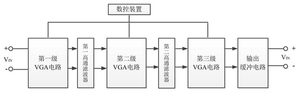
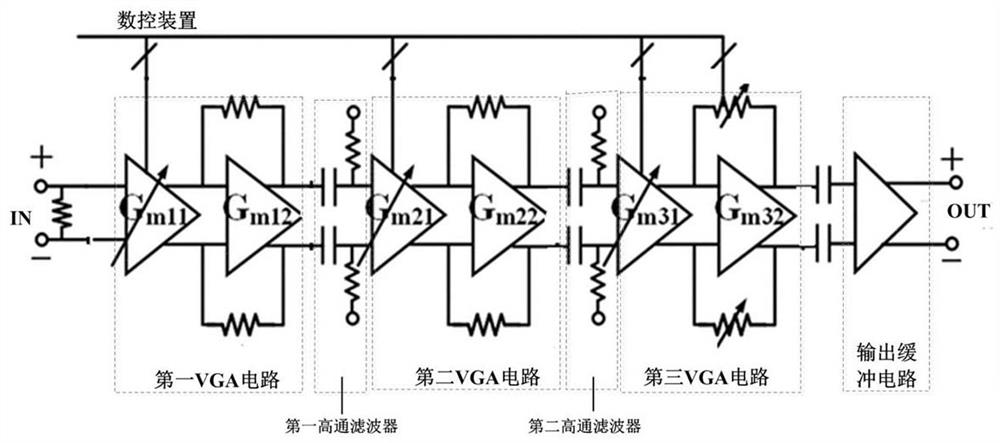
[0043] The present invention is based on the improved Cherry-Hooper amplifier gain unit. In the three-stage VGA circuit, the first and second stages are composed of a variable transconductance amplifier and a constant transimpedance amplifier, and the third stage is composed of a variable transconductance amplifier and a variable transimpedance amplifier. Composition, a high-pass filter is used between the two VGA circuits to eliminate the DC bias voltage generated by each VGA unit to ensure the reliability of the circuit, and the output buffer is used to drive a 100Ω differential load impedance.
[0044] like Figure 1-2 As shown, the digitally controlled variable gain amplifier among the present invention includes the first stage VGA circuit, the second stage VGA circuit, the third stage VGA circuit and the output buffer circuit connected in sequence;
[0045]The first input end and the second input end of the first-stage VGA circuit are jointly used as the input end of the ...
Embodiment 2
[0064] This embodiment provides the working principles of VGA circuits at all levels in the above embodiment 1:
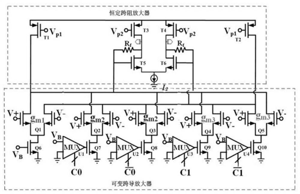
[0065] like image 3 As shown, the transconductances of the five input-pair transistors in the first-stage VGA circuit are g m1 , g m2 , g m2ˊ , g m3 , g m3ˊ , g m2 and g m2ˊ have the same transconductance value, but opposite polarity, when the digital control signal of the numerical control device is input into C 0 When the data selector controls the MOS switch to select the transconductance pair g m2 ; When the digital control signal input C 0 Non-time, through the data selector to control the MOS switch to select the transconductance pair g m2ˊ , g m3 and g m3ˊ Right works and g m2 and g m2ˊ for the same, when the digital control signal input C 1 When the data selector controls the MOS switch to select the transconductance pair g m3 ; When the digital control signal of the numerical control device is input into C 1 Non-time, through the data sele...
Embodiment 3
[0069] The digitally controlled variable gain amplifier in this embodiment has a 0.5-dB step size and a constant bandwidth. By using a variable transconductance stage and a variable transimpedance stage, a constant bandwidth exceeding 3.5 GHz is achieved. The subsequent simulation results are as follows Figure 5 As shown; the high gain above 60dB, the gain range of 30.5dB, the precise gain step size of 0.5dB, the maximum step size error between the simulation result and the design value (0.5dB) is less than ±0.15dB, such as Image 6 shown.
PUM
 Abstract
Description
Claims
Application Information