Novel heterojunction photoelectric device based on perovskite and preparation method thereof

A photoelectric device, perovskite technology, applied in the field of new heterojunction photoelectric devices based on perovskite and its preparation, can solve the problems of limiting perovskite research, poor detection and external quantum efficiency, and difficult photoelectric characteristics , to achieve the effect of great application potential, simple production and low cost

Pending Publication Date: 2020-11-06
SHANDONG UNIV
View PDF0 Cites 3 Cited by
  • Summary
  • Abstract
  • Description
  • Claims
  • Application Information

AI Technical Summary

Problems solved by technology

[0003] Generally speaking, the development of perovskite in the field of electronics is affected by its own characteristics, and it is difficult to have a considerable current value, so it will be more difficult to...

Method used


Image

  • Novel heterojunction photoelectric device based on perovskite and preparation method thereof
  • Novel heterojunction photoelectric device based on perovskite and preparation method thereof
  • Novel heterojunction photoelectric device based on perovskite and preparation method thereof

Examples


preparation example Construction

[0039] A method for preparing a novel heterojunction photoelectric device based on perovskite, comprising the following steps:

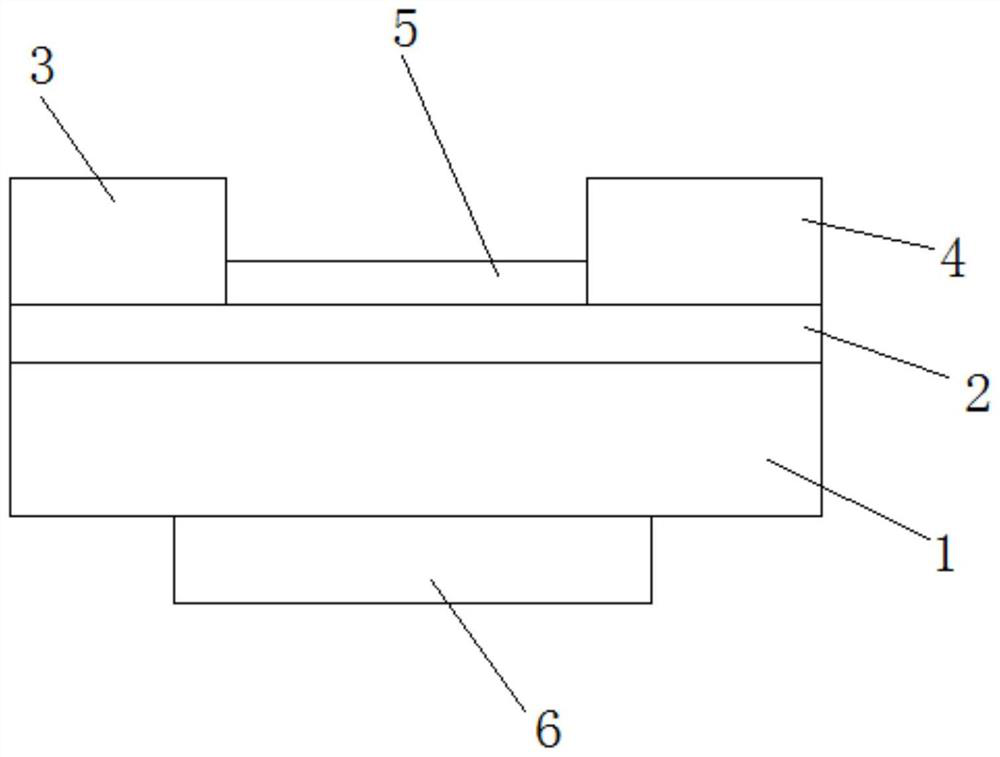
[0040] (1) in 1×1cm 2 Highly doped p-type Si is used as the substrate, and after being ultrasonically cleaned in acetone for 10 minutes, and then alternately washed with ethanol and deionized water for 3 times, a high-conductivity semiconductor substrate 1 is obtained;

[0041] (2) A layer of HfO is grown on the surface of the high-conductivity semiconductor substrate 1 by atomic layer deposition (ALD) 2 layer, the thickness of which is about 20nm;

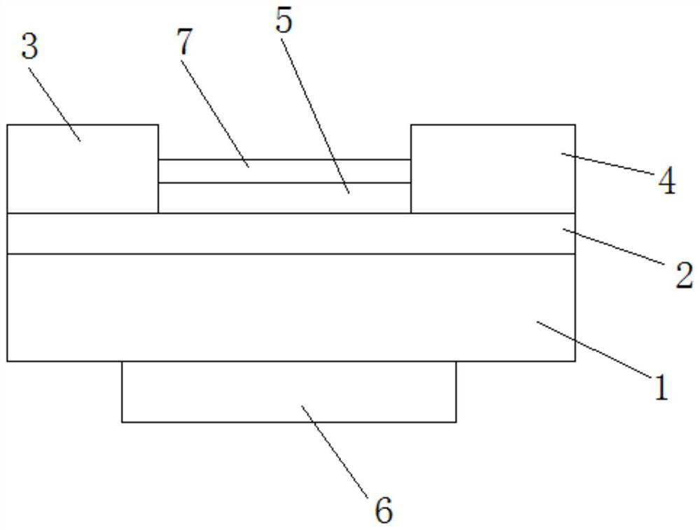
[0042] (3) Design the pattern of the source electrode 3 and the drain electrode 4 and the length of the channel through the mask plate, and the HfO 2 A source electrode 3 and a drain electrode 4 of Ti / Au material are deposited on the layer;

[0043] (4) by CsAc solution and PbBr 2 The solution is mixed according to the molar ratio of 1:4, and the reaction will proceed immediately to form perovskite C...


PUM

PropertyMeasurementUnit
Thicknessaaaaaaaaaa

Abstract

The invention discloses a novel heterojunction photoelectric device based on perovskite and a preparation method thereof. The photoelectric device comprises a semiconductor substrate and a hafnium dioxide layer located on the upper surface of the semiconductor substrate, a source electrode and a drain electrode are arranged on the upper surface of the hafnium dioxide layer, a perovskite film is arranged on the upper surface of the hafnium dioxide layer and located between the source electrode and the drain electrode, and a gate electrode is arranged on the lower surface of the semiconductor substrate. The photoelectric device disclosed by the invention has the advantages of small size, low cost, high performance, simplicity in manufacturing, high detection sensitivity and ultrahigh external quantum efficiency, and has great application potential in the field of photoelectric devices.

Description

technical field [0001] The invention relates to a photoelectric device, in particular to a novel heterojunction photoelectric device based on perovskite and a preparation method thereof. Background technique [0002] As one of the most popular materials in recent years, perovskite has successfully triggered a new round of research boom. Various perovskite materials such as organic-inorganic hybrid perovskite and all-inorganic perovskite have attracted the research interests of many researchers in the fields of photovoltaics, optoelectronics, and thermoelectricity, and their growth process is relatively simple and has higher stability. , and thus has received extensive attention. The quantum yield of some perovskites is as high as 90%, with suitable band gap and narrow line width of photoluminescence (PL) emission spectrum, so it can be used in optoelectronic fields, such as solar cells, LEDs, photodetectors, etc. . Moreover, the lower carrier recombination speed will also...

Claims


Application Information

Patent Timeline
IPC IPC(8): H01L51/42H01L51/44H01L51/48H01L31/0224H01L31/113H01L31/18
CPCH01L31/0224H01L31/1136H01L31/18H10K30/10H10K30/81H10K30/88Y02E10/549Y02P70/50
Inventor 张宇王彦皓韩琳
Owner SHANDONG UNIV
Why Eureka
Try Eureka