Broadband metamaterial absorber compatible with CMOS process

An absorber and metamaterial technology, which can be used in instruments, optics, nonlinear optics, etc., can solve the problems of limited bandwidth and total bandwidth, and achieve the effects of convenient fabrication, simple structure and reduced fabrication cost.

Inactive Publication Date: 2020-11-13
SOUTHEAST UNIV
View PDF6 Cites 2 Cited by
  • Summary
  • Abstract
  • Description
  • Claims
  • Application Information

AI Technical Summary

Problems solved by technology

Although various perfect absorbers utilizing plasmonic nanoresonators have been demonstrated, it is difficult to maintain large absorption over a wide wavelength range due to the limited bandwidth of plasmonic resonances
Multiband absorptio

Method used


Image

  • Broadband metamaterial absorber compatible with CMOS process
  • Broadband metamaterial absorber compatible with CMOS process
  • Broadband metamaterial absorber compatible with CMOS process

Examples


Embodiment 1

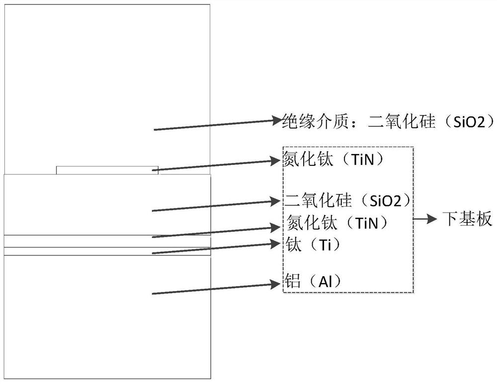
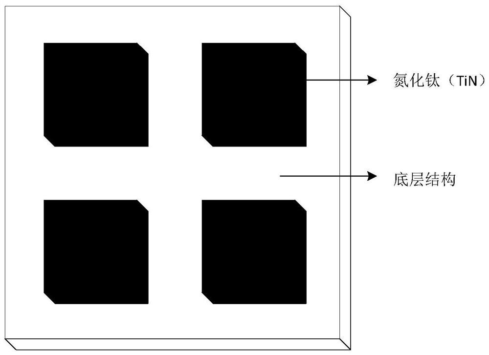
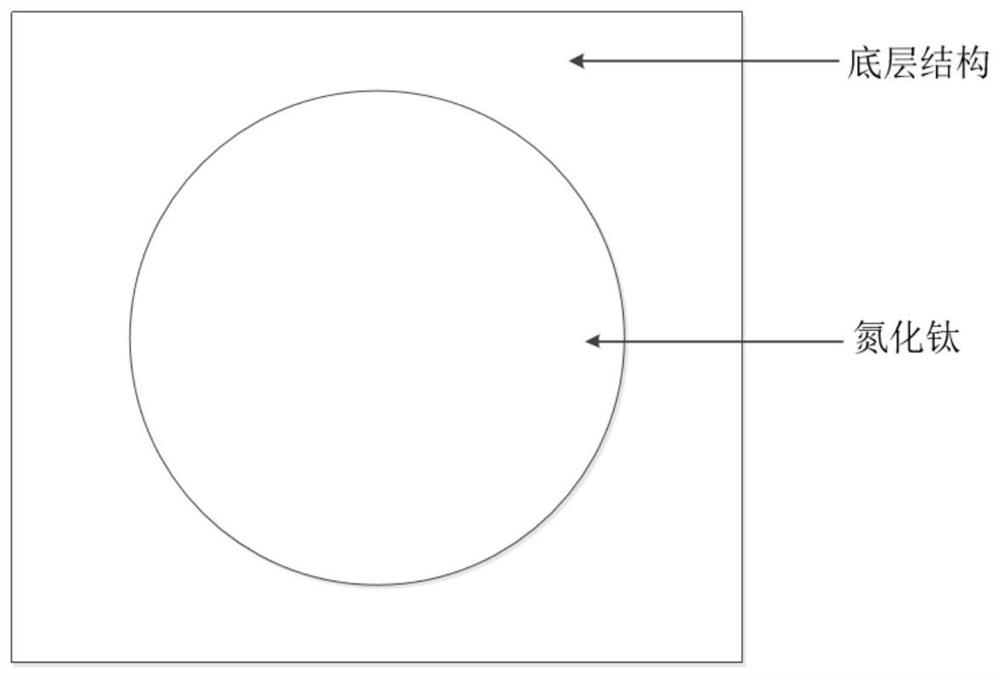
[0022] Embodiment 1: see figure 1 , a metamaterial absorber compatible with CMOS technology disclosed in the embodiment of the present invention can realize a wide range of high absorption rate functions in the visible light and optical communication bands. The metasurface absorber adopts a MIM structure to realize compatibility with CMOS technology and broadband absorption in the visible light band and the 1550nm optical communication band. The metasurface absorber of the present invention is based on the principle of surface plasmon resonance. Under the irradiation of incident light, the surface of the metal nanostructure generates induced charges, and the surface charges cause the collective oscillation of free electrons to generate surface plasmon resonance. , resulting in near-field enhancement around the metal structure and strong optical scattering and absorption resonance phenomena. Surface plasmons originate from the resonant oscillation generated by the mutual excit...


PUM


Abstract

The invention relates to a broadband metamaterial absorber compatible with a CMOS (Complementary Metal Oxide Semiconductor) process. The main structure of the metamaterial absorber comprises a lower substrate and an insulating medium which are arranged in sequence. The lower substrate comprises an MIM structure with a visible light waveband and 1550nm optical communication waveband super-absorption function. According to the invention, a broadband metasurface absorption structure compatible with a CMOS process can be realized, and a wide-range high-absorptivity function can be realized in visible light and optical communication wavebands.

Description

technical field [0001] The invention relates to an absorber, in particular to a wide-band metamaterial absorber compatible with CMOS technology, and belongs to the technical field of optical devices. Background technique [0002] Metamaterials refer to a class of artificial materials that do not exist in nature and have special properties. They have properties that traditional materials do not have, and can achieve functions that infectious materials cannot achieve. Metamaterials have shown powerful and versatile capabilities in controlling the absorption, reflection, and propagation of electromagnetic waves. They have inspired amazing designs and devices, including a perfect lens, black holes, plasmonic sensors, novel solar energy harvesting concepts and more. Among them, the performance of metamaterial absorbers is related to the constituent materials and their unit structure and size, with near-perfect absorption, deep subwavelength thickness, and tunability. In the opt...

Claims


Application Information

Patent Timeline
IPC IPC(8): G02B5/00G02F1/1335G02B1/00
CPCG02B1/002G02B5/003G02B5/008G02F1/133512
Inventor 张易晨夏军
Owner SOUTHEAST UNIV
Why Eureka
Try Eureka