Chip welding structure and welding method

A chip welding and chip technology, applied in the field of chip welding structure and welding, can solve the problems of chip internal structure damage, high packaging cost, large chip impact, etc., and achieve the effect of reducing impact force, production cost, and impact force.

Pending Publication Date: 2020-11-13
CHIPMOS TECHSHANGHAI
View PDF9 Cites 1 Cited by
  • Summary
  • Abstract
  • Description
  • Claims
  • Application Information

AI Technical Summary

Problems solved by technology

[0004] In the prior art, the connection between the chip (chip) and the substrate is completed by welding with a metal wire (bonding wire), which may cause high packaging costs, or a large impact on the chip during packaging, causing the chip to fail due to internal structure damage. Failure and other issues

Method used


Image

  • Chip welding structure and welding method
  • Chip welding structure and welding method
  • Chip welding structure and welding method

Examples


Embodiment 1

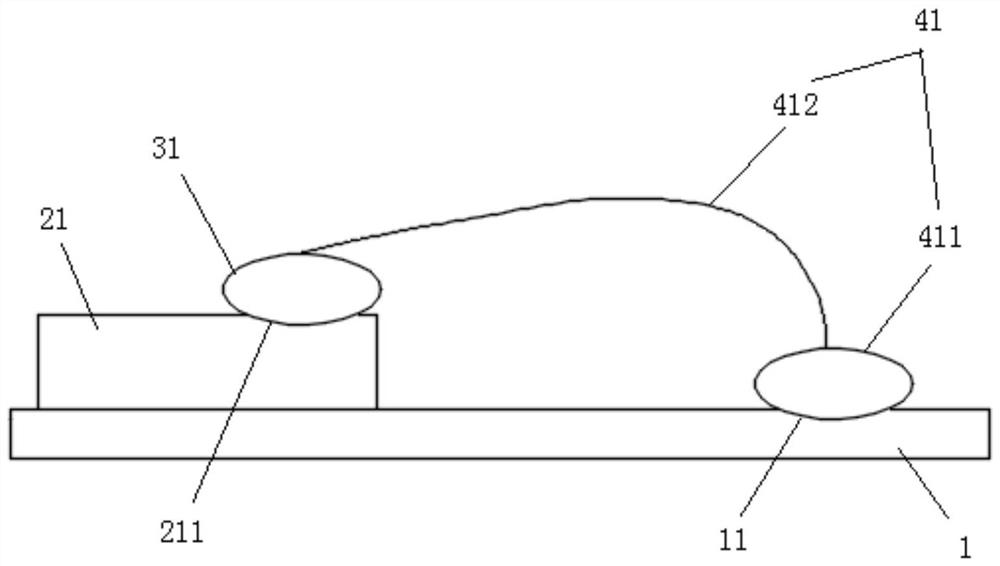
[0043] Such as figure 1 , figure 2 As shown, the chip bonding structure of this embodiment realizes the electrical connection between a single chip and the substrate, including: the substrate 1 , the first chip 21 , the first gold pad 31 and the first copper connection wire 41 .

[0044] The first chip 21 is disposed on the upper surface of the substrate 1 .

[0045] The first gold pad 31 is disposed on the upper surface of the first chip 21 , and the first gold pad 31 is located at one end of the first chip 21 .

[0046] The first copper connection line 41 includes: a first copper welding point 411 and a first copper welding line 412 .

[0047] The first copper pad 411 is located at one end of the first copper wire 412, and the other end of the first copper pad 411 and the first copper wire 412 are connected to the first gold pad 31 on the first chip 21 and the substrate 1 respectively. The connection is through the first copper pad 411 and the first copper wire 412 , so ...

Embodiment 2

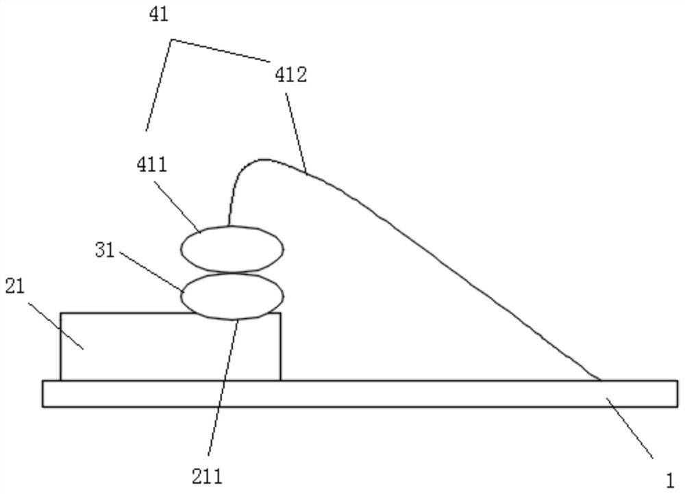
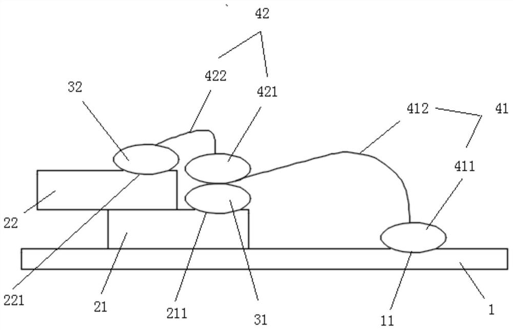
[0055] optional, such as image 3 , Figure 4 As shown, the chip bonding structure of this embodiment realizes the electrical connection between multiple chips and the substrate. In this embodiment, it also includes: a second chip 22 , a second gold pad 32 and a second copper connection wire 42 .

[0056] The second chip 22 is dislocated and stacked on the first chip 21 , a step is formed between the second chip 22 and the first chip 21 , and the first gold pad 31 on the first chip 21 is set at the step.

[0057] The second gold pad 32 is disposed at one end of the second chip 22 , and the second gold pad 32 is located at one end close to the first gold pad 31 .

[0058] The second copper connection line 42 includes: a second copper welding point 421 and a second copper welding line 422 .

[0059] The second copper pad 421 of the second copper connection wire 42 is located at one end of the second copper pad 422, and the second copper pad 421 and the other end of the second ...

Embodiment 3

[0068] This embodiment provides a welding method for realizing a chip welding structure, including the following steps:

[0069] S1. Use a wire bonding machine to respectively weld first gold pads and second gold pads on the first chip and the second chip with gold wires.

[0070] S2. Using a wire bonding machine, copper wires are used to electrically connect the second gold soldering point to the first gold soldering point, and to electrically connect the first gold soldering point to the substrate.

[0071] Specifically, when the chip is connected to the substrate, use a wire bonding machine to first use gold wires to weld gold solder joints on the chip respectively, and if it is a multi-layer chip stacked in a multi-layer dislocation, solder the chips on each layer separately. Gold solder joints.

[0072] Then copper wires are used to connect the gold pads on the chips of each layer to the substrate in sequence. When connecting copper wires, if the space permits, use the ...


PUM


Abstract

The invention relates to the field of semiconductor packaging, and discloses a chip welding structure and a welding method. The chip welding structure comprises a substrate, a first chip, a first goldwelding spot and a first copper connecting wire, wherein the first chip is arranged on the substrate, the first gold welding spot is arranged on the first chip, and the two ends of the first copper connecting wire are connected with the first chip and the substrate respectively. According to the chip welding structure, a gold welding spot is formed on the chip by using a gold wire made of a softmaterial, impact force on the chip is small, and the internal structure of the chip is not easy to damage; a copper wire is adopted to form the first copper connecting wire, the two ends of the firstcopper connecting wire are connected with the gold welding spot and the substrate respectively, so that the chip and the substrate are electrically communicated; and due to buffering of the gold welding spot, impact force on the chip during copper wire welding is effectively reduced, it is guaranteed that the chip structure is not damaged, and meanwhile, the production cost during chip packaging is reduced.

Description

technical field [0001] Embodiments of the present invention relate to the field of semiconductor packaging, and in particular to a chip bonding structure and a bonding method. Background technique [0002] Semiconductor packaging refers to the process of processing the tested wafers according to the product model and functional requirements to obtain independent chips. The packaging process is: the wafer from the wafer front-end process is cut into small chips (Die) after the dicing process, and then the cut chip is mounted on the corresponding substrate frame (Die) with silver glue or adhesive tape (DAF) Lead frame) on the small island, and then use ultra-fine metal (gold, silver, copper and aluminum) wires (bonding wires) to connect the bonding pads (Bond Pad) of the chip to the corresponding pins (Lead) of the substrate, and form the required circuit. [0003] The metal wire (bonding wire) is fixed on the substrate and the chip (chip) by a wire bonding machine, so that ...

Claims


Application Information

Patent Timeline
IPC IPC(8): H01L23/488H01L23/49H01L21/48H01L21/60
CPCH01L23/488H01L23/49H01L21/4846H01L24/49H01L2224/48471H01L2224/48465H01L2224/48145H01L2224/48479H01L2224/48482H01L2224/48091H01L2924/00014
Inventor 蒋以青陈晟童璐晟邵兹人
Owner CHIPMOS TECHSHANGHAI
Why Eureka
Try Eureka