Silicon carbide crystal growth method and device

A technology of crystal growth and silicon carbide, applied in the directions of crystal growth, single crystal growth, single crystal growth, etc., can solve the problems affecting crystal crystallization quality, affecting crystal quality, seed crystal nucleation, etc., to improve quality, avoid sublimation, avoid The effect of pollution

Active Publication Date: 2020-11-17
SICC CO LTD
View PDF7 Cites 2 Cited by
  • Summary
  • Abstract
  • Description
  • Claims
  • Application Information

AI Technical Summary

Problems solved by technology

Unstable atmosphere transmission will affect the nucleation of silicon carbide atmosphere on the seed crystal, which can easily induce defects such as polymorphism and dislocation, which will affect the quality of crystallization
At the same time, some impurities in the powder will be sublimated below the growth temperature of silicon carbide, and the transfer to the surface of the seed crystal will induce nucleation problems
The silicon carbide crystal growth methods and devices in the prior art cannot completely block the upward transportation of the silicon carbide atmosphere in the early stage of crystal growth, thereby affecting the nucleation of the silicon carbide atmosphere on the seed crystal, which easily induces defects such as polymorphism and dislocation, and affects the crystal. the quality of

Method used


Image

  • Silicon carbide crystal growth method and device
  • Silicon carbide crystal growth method and device
  • Silicon carbide crystal growth method and device

Examples


Embodiment 1

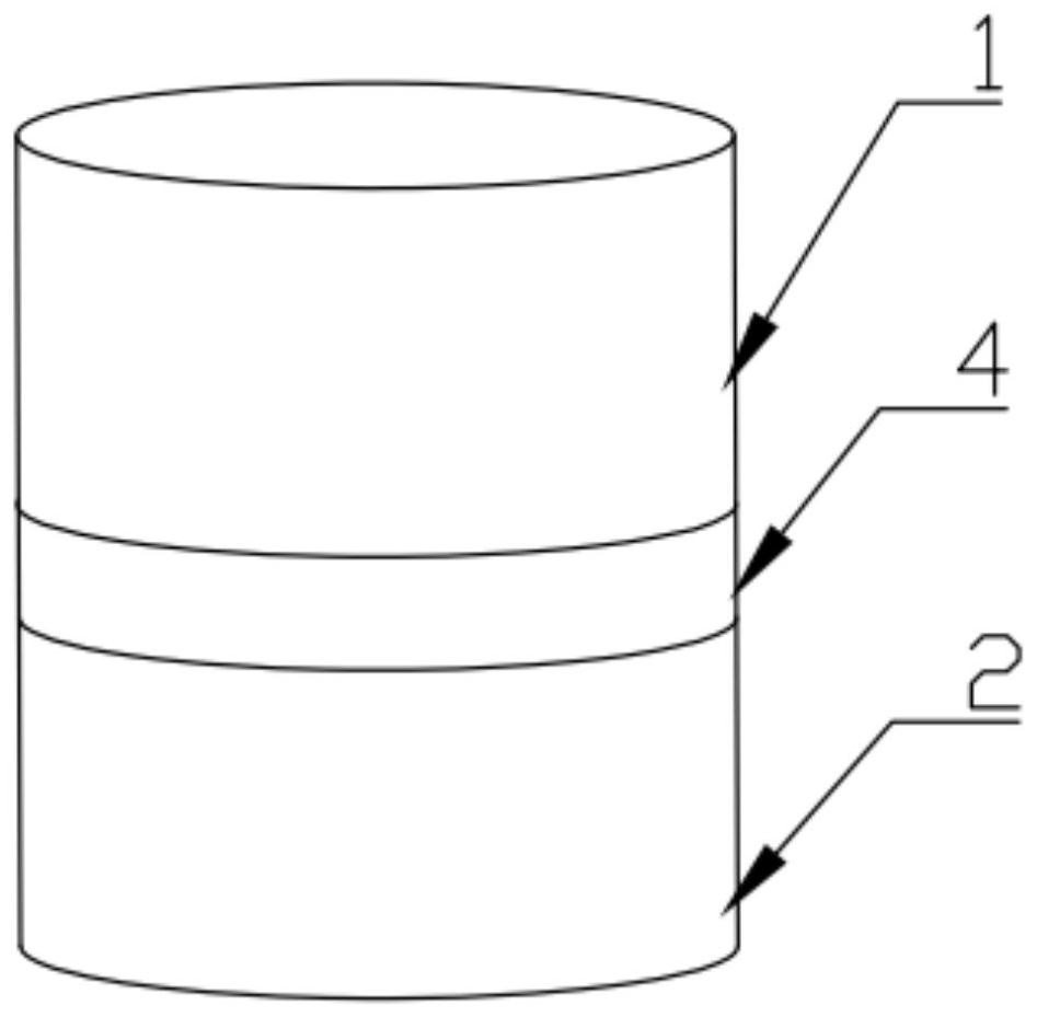
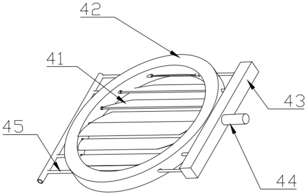
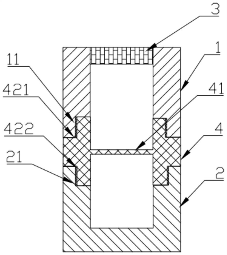
[0047] refer to Figure 1-3 , the present embodiment provides a device for growing silicon carbide crystals, the device includes a first crucible 1, a second crucible 2 and a heating device, the first crucible 1 is cylindrical with two ends open, and the second crucible 2 is arranged above There is a crucible cover 3; the second crucible 2 is cylindrical with one end open, and the second crucible 2 is located below the first crucible 1; the first crucible 1 and the second crucible 2 are connected to form an internal cavity, and a partition 41 is arranged in the cavity A plurality of partitions 41 rotate to no gap between the plurality of partitions 41 and between the partitions 41 and the cavity inner wall, then a plurality of partitions 41 cut off the first crucible 1 and the second crucible 2; a plurality of partitions 41 rotate When there are gaps between the plurality of partitions 41 and / or between the partitions 41 and the cavity, the first crucible 1 communicates with t...

Embodiment 2

[0061] In a specific embodiment, there is provided a method for preparing silicon carbide crystals using the above-mentioned silicon carbide crystal device, the method comprising the following steps:

[0062] (1) Assembly stage: bond the seed crystal on the top of the first crucible, place the silicon carbide raw material at the bottom of the second crucible, connect the first crucible and the second crucible to form an internal cavity, and set a plurality of rotatable partitions in the cavity plate;

[0063] (2) Heating and heating stage: place the assembled first crucible and second crucible in the crystal growth furnace, vacuumize the crystal growth furnace, and control the rotation of multiple partitions between the plurality of partitions and between the partitions and the There is no gap between the inner walls of the cavity, so that the first crucible is separated from the second crucible,

[0064] Heating to 1200-1800°C, and introducing protective gas, the pressure is...


PUM


Abstract

The invention provides a silicon carbide crystal growth method and device. The method comprises the steps: (1) an assembly stage; (2) a sublimation stage: controlling a plurality of separation platesto rotate until there is no gap between the plurality of separation plates and between the separation plates and the inner wall of a cavity, separating a first crucible from a second crucible, and heating to sublimate a silicon carbide raw material; and (3) a crystal growth stage: controlling the plurality of separation plates to rotate until a gap exists between the plurality of separation platesand / or between the separation plate and the inner wall of the cavity, communicating the second crucible with the first crucible through the gap, and heating to enable the silicon carbide raw materialatmosphere to pass through the gap to be transmitted to the seed crystal for crystal growth. By controlling rotation of the multiple separation plates, the first crucible and the second crucible areseparated, the sublimated atmosphere of the silicon carbide raw material cannot be conveyed upwards, the defect that the crystal quality is affected and seed crystals are damaged and polluted due to the fact that the unstable atmosphere is formed in the early growth stage is overcome, and the separation plates block heat radiation of the raw material to the seed crystals, so that the sublimation of the surface of the seed crystal caused by no silicon carbide atmosphere supplement during impurity removal is avoided.

Description

technical field [0001] The invention relates to a silicon carbide crystal growth method and device, belonging to the technical field of silicon carbide crystal growth. Background technique [0002] Silicon carbide (SiC) crystals have excellent semiconductor physical properties such as high thermal conductivity, high breakdown voltage, extremely high carrier mobility, and high chemical stability. They can be made into high-frequency, High-power electronic devices and optoelectronic devices have great application value in the fields of national defense, high technology, industrial production, power supply, and power transformation, and are regarded as the third-generation wide-bandgap semiconductor materials with great development prospects. [0003] The growth process of silicon carbide crystals grown by PVT method is carried out in a closed graphite crucible. The silicon carbide powder (or silicon, carbon solid mixture) as the growth source is placed at the bottom of the cru...

Claims


Application Information

Patent Timeline
Patent Type & Authority Applications(China)
IPC IPC(8): C30B23/00C30B29/36
CPCC30B23/002C30B29/36
Inventor 舒天宇王宗玉梁庆瑞张红岩姜岩鹏
Owner SICC CO LTD
Why Eureka
Try Eureka