High-voltage three-dimensional depletion super-junction LDMOS device and manufacturing method thereof

A manufacturing method and three-dimensional technology, applied in semiconductor/solid-state device manufacturing, semiconductor devices, electrical components, etc., to achieve the effect of increasing doping concentration and ensuring device withstand voltage

Pending Publication Date: 2020-11-20
UNIV OF ELECTRONICS SCI & TECH OF CHINA
View PDF11 Cites 7 Cited by
  • Summary
  • Abstract
  • Description
  • Claims
  • Application Information

AI Technical Summary

Problems solved by technology

However, the drift region of the conventional superjunction and RESURF technology only comes from the auxiliary depletion of the charge compensation layer on both sides, and its improvement of device performance is getting closer and closer to the limit. How to further increase the compensation ability of the charge compensation layer and improve the doping of the drift region The impurity concentration, to further reduce the specific on-resistance while ensuring the withstand voltage, is the core issue of device improvement.

Method used


Image

  • High-voltage three-dimensional depletion super-junction LDMOS device and manufacturing method thereof
  • High-voltage three-dimensional depletion super-junction LDMOS device and manufacturing method thereof
  • High-voltage three-dimensional depletion super-junction LDMOS device and manufacturing method thereof

Examples


Embodiment 1

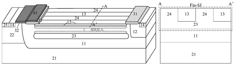
[0040] Such as figure 1 Shown is a schematic structural diagram and a cross-sectional view of a high-voltage three-dimensional depleted superjunction LDMOS device according to Embodiment 1 of the present invention, specifically including: a substrate 21 of a second conductivity type, a drift region 11 of a first conductivity type, and a well region 12 of a first conductivity type and the second conductivity type well region 22, the first dielectric oxide layer 31, the second dielectric oxide layer 32, the second conductivity type buried layer 23, the first conductivity type regions 13 and the second conductivity type regions 24 arranged periodically, and Doping the first conductivity type region 14 and heavily doping the second conductivity type region 25, control gate polysilicon 41;

[0041] Wherein, the well region 12 of the first conductivity type is located on the right side of the drift region 11 of the first conductivity type, the well region 22 of the second conductivi...

Embodiment 1

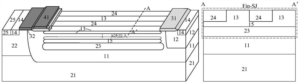
[0060] Such as figure 2 Shown is a schematic structural diagram and a cross-sectional view of the high-voltage three-dimensional depleted superjunction LDMOS device in Example 2 of the present invention, which is implanted into the buried layer of the first conductive type after the implantation of the buried layer 23 of the second conductive type in the manufacturing step 4 of the implementation example 1 15, and at the same time push the junction to form, the subsequent first conductivity type region 13 and the second conductivity type region 24 are implanted and connected to the first conductivity type buried layer 15, the dose and times of super junction implantation required in this embodiment are reduced, and the subsequent The process steps remain the same. The buried layer 15 of the first conductivity type and the region 13 of the first conductivity type surround the region 23 of the second conductivity type in three directions, forming a three-dimensional depleted su...

Embodiment 3

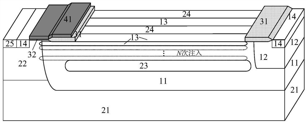
[0062] Figure 3(a) is a schematic structural diagram of a high-voltage three-dimensional depleted superjunction LDMOS device in Example 3 of the present invention. In this example, the superjunction source is implanted into the second conductivity type well region 22 on the basis of Example 1. In this process, the grounding of the second conductivity type region 24 is realized to improve the dynamic characteristics of the device. As shown in FIG. 3( b ), it is a schematic diagram of another modified structure of Embodiment 3 of the present invention. The superjunction second conductivity type region 24 is introduced into the source end heavily doped first conductivity type region 14 and heavily doped second conductivity type region 25 along the first conductivity type drift region 11 and the second conductivity type well region 22 , the super-junction first conductivity type region 13 remains unchanged to realize super-junction grounding, and the rest of the working principles ...


PUM


Abstract

The invention provides a high-voltage three-dimensional depletion super-junction LDMOS and a manufacturing method thereof. The high-voltage three-dimensional depletion super-junction LDMOS comprises asecond conductive type substrate, a first conductive type drift region, a first conductive type well region, a second conductive type well region, a first dielectric oxide layer, a second conductivetype buried layer, a second dielectric oxide layer, and a first conductive type region and a second conductive type region which form a super junction, wherein the second conductive type buried layerand the super junction structure are both located in the first conductive type drift region, and the super junction is located above the second conductive type buried layer and connected with the second conductive type buried layer; the second conductive type buried layer optimizes the surface electric field of the device in an off state; the second conductive type buried layer and the super-junction second conductive type region surround the super-junction first conductive type region from three sides to form a three-dimensional depletion super-junction structure Fin-SJ structure, the dopingconcentration of the first conductive type drift region and the super-junction first conductive type region is allowed to be improved, the super-junction structure provides a surface low-resistance path, and the specific on-resistance of the device is reduced.

Description

technical field [0001] The invention belongs to the technical field of semiconductor process manufacturing, and in particular relates to a novel high-voltage three-dimensional depletion superjunction LDMOS device (Fin-SJ LDMOS device) and a manufacturing method thereof. Background technique [0002] Because of its high input impedance, low loss, fast switching speed, wide safe operating area and easy integration, high-voltage LDMOS has always been used as a core device in power integrated circuits, and is widely used in mobile communications, automotive electronics, LED lighting, etc. in the field. The performance of high-voltage LDMOS often requires that it can withstand high voltage while reducing the specific on-resistance as much as possible. In order to achieve this goal, the existing commonly used technologies include lateral superjunction and surface field reduction (RESURF) technology, all of which are passed in the drift region. The opposite charge compensation lay...

Claims


Application Information

Patent Timeline
Patent Type & Authority Applications(China)
IPC IPC(8): H01L29/06H01L29/78H01L21/336
CPCH01L29/0623H01L29/0634H01L29/7823H01L29/66681H01L29/7835H01L29/42368
Inventor 张波朱旭晗祖健章文通乔明李肇基
Owner UNIV OF ELECTRONICS SCI & TECH OF CHINA
Why Eureka
Try Eureka