Active clamping circuit of IGBT
A technology of clamping circuit and push-pull circuit, which is applied in the direction of electrical components, output power conversion devices, etc., can solve the problems of exceeding the IGBT breakdown voltage point and the large peak of the IGBT turn-off voltage, and achieve a small clamping action voltage range Effect
- Summary
- Abstract
- Description
- Claims
- Application Information
AI Technical Summary
Problems solved by technology
Method used
Image
Examples
Embodiment Construction
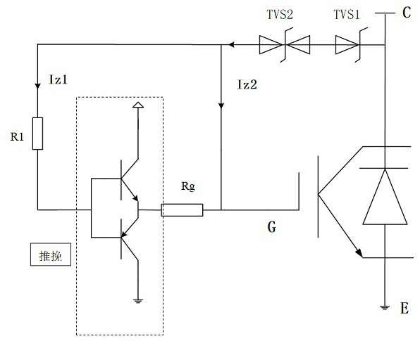
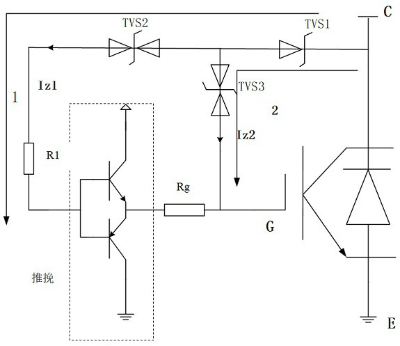
[0018] Such as figure 2 As shown in the active clamping circuit of the IGBT of the present invention, the gate G of the IGBT is connected with the drive resistor of the push-pull circuit, the collector C and the emitter E of the IGBT are connected to the high level and the ground respectively, and the push-pull The pull circuit is composed of two common base push-pull transistors, and the output end of the push-pull circuit is connected to the gate G of the IGBT through the drive resistor Rg.
[0019] figure 2 Among them, the active clamping circuit includes three transient voltage suppression diodes: unidirectional TVS1, bidirectional TVS2 and bidirectional TVS3; the cathode of TVS1 is connected to the collector C of the IGBT, and the anode of TVS1 is respectively connected to TVS2, One end of TVS3, the other end of TVS2 and TVS3 are respectively connected to the base of the push-pull circuit and the gate G of the IGBT.
[0020] In view of the large gate capacitance of th...
PUM
 Abstract
Description
Claims
Application Information
 - R&D Engineer
- R&D Manager
- IP Professional
- Industry Leading Data Capabilities
- Powerful AI technology
- Patent DNA Extraction
Browse by: Latest US Patents, China's latest patents, Technical Efficacy Thesaurus, Application Domain, Technology Topic, Popular Technical Reports.
© 2024 PatSnap. All rights reserved.Legal|Privacy policy|Modern Slavery Act Transparency Statement|Sitemap|About US| Contact US: help@patsnap.com


