Anti-dv/dt SGT device

A device and conductivity type technology, applied in the field of SGT devices, can solve the problems of increasing the possibility of voltage shock dv/dt failure of devices, electromagnetic pollution of components and equipment, and turning on of parasitic transistors, so as to reduce Miller capacitance Cgd and reduce EMI electromagnetic radiation noise and the effect of reducing switching oscillation

Pending Publication Date: 2020-11-24
VANGUARD SEMICON CORP
View PDF0 Cites 0 Cited by
  • Summary
  • Abstract
  • Description
  • Claims
  • Application Information

AI Technical Summary

Problems solved by technology

When it is used as a power switch tube to control energy flow and conversion, it works in a fast switching transition state, facing a high voltage oscillation dv / dt and current oscillation di / dt between the drain and source, on the one hand the high The voltage shock dv / dt is superimposed on the device, which is easy to cause the parasitic transistor to turn on and cause the device to fail; on the other hand, the high voltage shock dv / dt is superimposed in the switching system, causing great electromagnetic interference, thus affecting the surrounding components and The equipment produces serious electromagnetic pollution
[0003] The existing SGT-MOSFET connects the shielded gate to the source potential, increases the switching speed and reduces the switching loss by reducing the Miller capacitance Cgd of the device, which inevitably leads to greater voltage oscillation dv / dt and The current oscillates di / dt, thereby increasing the possibility of device voltage oscillating dv / dt failure

Method used


Image

  • Anti-dv/dt SGT device
  • Anti-dv/dt SGT device
  • Anti-dv/dt SGT device

Examples


Embodiment Construction

[0042] The present invention will be described in detail below in conjunction with the accompanying drawings and specific embodiments.

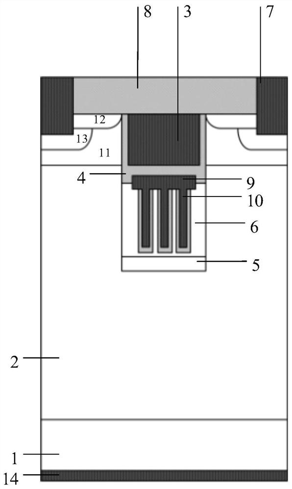
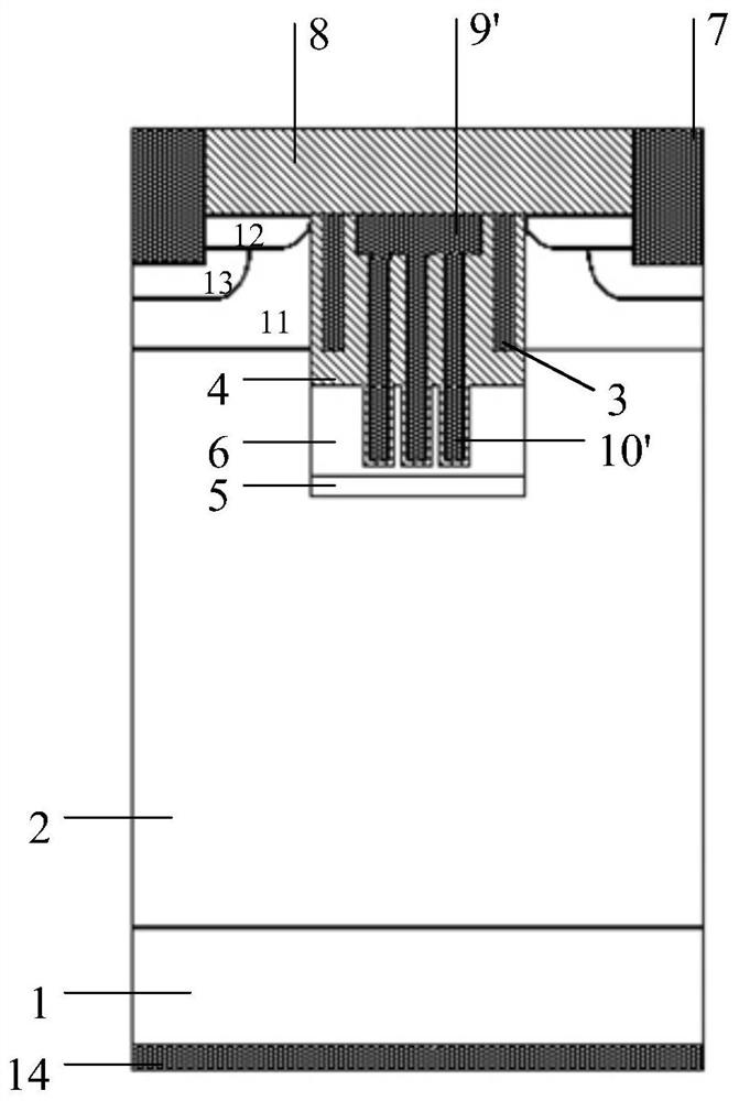
[0043] refer to Figures 1 to 3 As shown, the present invention provides a dv / dt resistant SGT device, comprising: a substrate 1 of the first conductivity type; an epitaxial layer 2 of the first conductivity type, located on the upper surface of the substrate 1 of the first conductivity type; The groove is located in the epitaxial layer 2 of the first conductivity type and extends along the thickness direction of the epitaxial layer 2 of the first conductivity type; the polysilicon gate 3 and the shielding gate are arranged in the groove; the first dielectric layer 4, Located on the bottom and side surfaces of the shielded gate, on the side of the polysilicon gate 3, and used to isolate the polysilicon gate 3 and the shielded gate; the lightly doped body region 5 of the first conductivity type is located at the bottom of the trench, and is lo...


PUM


Abstract

The invention discloses an anti-dv / dt SGT device, which comprises a substrate of a first conductive type, an epitaxial layer of the first conductive type positioned on the upper surface of the substrate of the first conductive type, a trench located in the epitaxial layer of the first conductive type, a first dielectric layer, a lightly doped body region of the first conductive type located at thebottom part of the trench, a heavily doped body region of the first conductive type located on the periphery of the first dielectric layer, source electrode metal located above the side face of the epitaxial layer of the first conductive type, a second dielectric layer located on the upper surface of the trench, and a polycrystalline silicon gate and a shielding gate which are positioned in the trench. According to the anti-dv / dt SGT device, the drain-source capacitance Cds can be increased, and the switching oscillation is reduced, so that the possibility of voltage oscillation dv / dt failureof the device is reduced.

Description

technical field [0001] The invention relates to the technical field of semiconductor devices, in particular to a dv / dt-resistant SGT device. Background technique [0002] Shielded Gate Trench MOSFET (SGT-MOSFET for short) power devices have been widely used in the prior art. At the same time, MOSFETs (Metal Oxide Semiconductor Field Effect Transistors) are widely used in various fields such as switching power supplies, automotive electronics, and motor drives due to their advantages of large input resistance, easy driving, simple control, and high frequency characteristics. When it is used as a power switch tube to control energy flow and conversion, it works in a fast switching transition state, facing a high voltage oscillation dv / dt and current oscillation di / dt between the drain and source, on the one hand the high The voltage shock dv / dt is superimposed on the device, which is easy to cause the parasitic transistor to turn on and cause the device to fail; on the other ...

Claims


Application Information

Patent Timeline
Patent Type & Authority Applications(China)
IPC IPC(8): H01L23/552H01L29/78H01L29/423
CPCH01L23/552H01L29/4236H01L29/7813
Inventor 郭乔林泳浩李伟聪
Owner VANGUARD SEMICON CORP
Why Eureka
Try Eureka