Anti-EMI super-junction VDMOS device and preparation method thereof
A device and conductive type technology, applied in the field of anti-EMI superjunction VDMOS devices and preparation, can solve the problems of electromagnetic pollution of components and equipment, parasitic transistor turn-on, fast switching speed, etc., to reduce EMI electromagnetic radiation noise, reduce switching The effect of shock and endurance improvement
- Summary
- Abstract
- Description
- Claims
- Application Information
AI Technical Summary
Problems solved by technology
Method used
Image
Examples
Embodiment 1
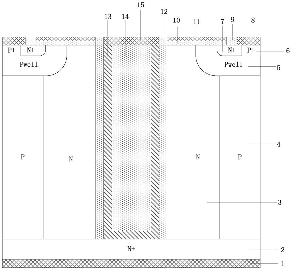
[0053] like figure 1 As shown, Embodiment 1 of the present invention provides a kind of anti-EMI super junction VDMOS device, comprising:
[0054] Drain Metal 1;
[0055] a substrate 2 of the first conductivity type located above the drain metal 1;
[0056] A super junction drift region located above the substrate 2 of the first conductivity type, the super junction drift region includes a drift region 3 of the first conductivity type and a drift region 4 of the second conductivity type;
[0057] The second conductivity type base region 5 located on the upper part of the superjunction drift region;
[0058] The second conductivity type ohmic contact region 6 and the first conductivity type source region 7 located inside the second conductivity type base region 5;
[0059] a gate oxide layer 10 located above the base region 5 of the second conductivity type;
[0060] a gate 11 located above the gate oxide layer 10;
[0061] The source metal 8 located above the second condu...
Embodiment 2
[0069] Embodiment 2 of the present invention provides a method for preparing an anti-EMI super junction VDMOS device, including the following process:
[0070] Take the semiconductor substrate material of the first conductivity type;
[0071] Epitaxially form the drift region of the super junction structure on the substrate material;
[0072] Etching a trench in the super junction drift region, the trench runs through the entire super junction drift region to the first conductivity type substrate;
[0073] growing an oxide layer dielectric on the sidewall of the trench;
[0074] Depositing and forming a U-shaped semi-insulating polysilicon layer in the trench;
[0075] Depositing an oxide layer dielectric in the U-shaped semi-insulating polysilicon layer;
[0076] growing a gate oxide over the drift region;
[0077] Depositing a polysilicon gate over the gate oxide;
[0078] Ion implantation in the upper part of the drift region and push the junction to form the base regi...
PUM
| Property | Measurement | Unit |
|---|---|---|
| thickness | aaaaa | aaaaa |
| thickness | aaaaa | aaaaa |
Abstract
Description
Claims
Application Information
