

Mask for photovoltaic cell and preparation method of mask
A technology of photovoltaic cells and manufacturing methods, which is applied in the manufacture of circuits, electrical components, and final products, can solve the problems of high cost, complicated photolithography technology, and difficulty in meeting the accuracy requirements of patterned masks, so as to simplify the process and reduce the cost. cost effect
- Summary
- Abstract
- Description
- Claims
- Application Information
AI Technical Summary
Problems solved by technology
Method used
Image

Examples
Embodiment 1
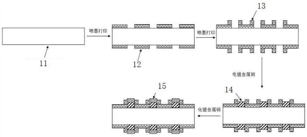
[0020] see figure 1 , making a patterned mask on the two surfaces of the semi-finished solar cell 11, the specific method steps are:
[0021] S11. Heat the wax whose melting temperature is between 40-150° C. to melt, and first print a layer of wax on the corresponding areas of the two surfaces of the solar cell by inkjet printing to form a patterned mask 12;
[0022] S12 , printing more wax at the opening edge position 13 of the patterned mask 12 to thicken it, so as to meet the height of the opening edge of the patterned mask, and save materials and process time. In some other embodiments, colorants or dyes are added to the wax to make it have a specific color, but ensure that the average photon transmittance of the mask is greater than 10 in the UV-VIS-NIR (ultraviolet-visible-near infrared) range. %.
[0023] S13 , depositing copper metal 14 in the opening area of the patterned mask by using an electroplating method, and then depositing tin metal 15 by using an electrol...
Embodiment 2
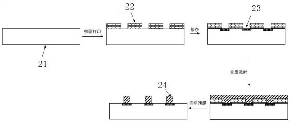
[0025] see figure 2 , making a patterned mask on the emitter surface of the semi-finished solar cell 21, the specific method steps are:
[0026] S21, heating the wax with a melting temperature between 40-150° C. to melt, and then printing a single layer or multiple layers of wax on the corresponding area of the surface of the solar cell by inkjet printing to form a patterned mask 22;
[0027] S22 , perform heavy doping on the solar cell in the opening region 23 of the patterned mask 22 , and then form metal grid lines 24 by sputtering metal in the mask opening above the heavily doped region.
[0028] S23. Finally, the solar cell is heated to a temperature above the melting temperature of the wax to melt it, and then the whole or part of the wax is removed from the solar cell by air flow or water flow. In some other embodiments, the wax forming the patterned mask is soluble in a specific acid, alkali or organic solvent, and can be removed with a corresponding acid, alkali o...
Embodiment 3
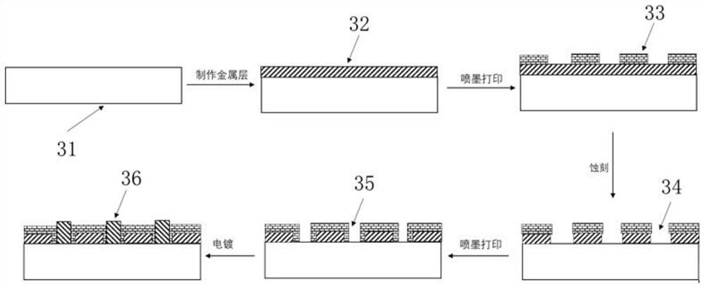
[0030] see image 3 , making a patterned mask on the surface of the semi-finished solar cell 31, the specific method steps are:
[0031] S31 , making positive electrode metal contact 32 on the surface of one end of semi-finished solar cell 31 by electroplating, screen printing, vacuum coating and other methods.
[0032] S32. Heat the wax with a melting temperature between 40-150°C until it melts, and then print a single layer or multiple layers of wax on the corresponding area of the solar cell by inkjet printing to form a patterned mask 33, the patterned mask The film 33 is insulating and has an average photon transmittance greater than 90% in the UV-VIS-NIR (ultraviolet-visible-near infrared) range.
[0033] S33 , etching away the anode metal contact 32 in the opening area 34 of the patterned mask 33 on the solar cell.
[0034] S34 , printing wax on the edge area of the opening of the patterned mask 33 by inkjet printing again, so that the metal contact of the positive...
PUM
| Property | Measurement | Unit |
|---|---|---|
| melting point | aaaaa | aaaaa |
Abstract
Description
Claims
Application Information