Printed circuit board and preparation method thereof
A printed circuit board and circuit board technology, applied in the directions of printed circuit manufacturing, printed circuit, multilayer circuit manufacturing, etc., can solve the problems of signal loss, residual piles, etc., to reduce signal loss, save costs, The effect of improving the quality of signal transmission
- Summary
- Abstract
- Description
- Claims
- Application Information
AI Technical Summary
Problems solved by technology
Method used
Image

Examples
no. 1 example
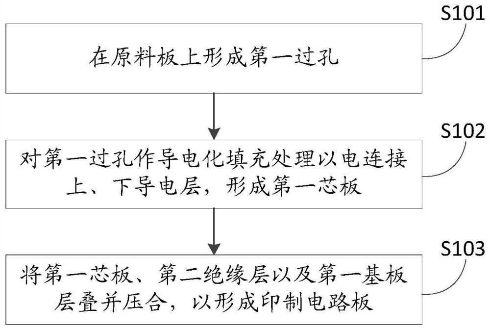
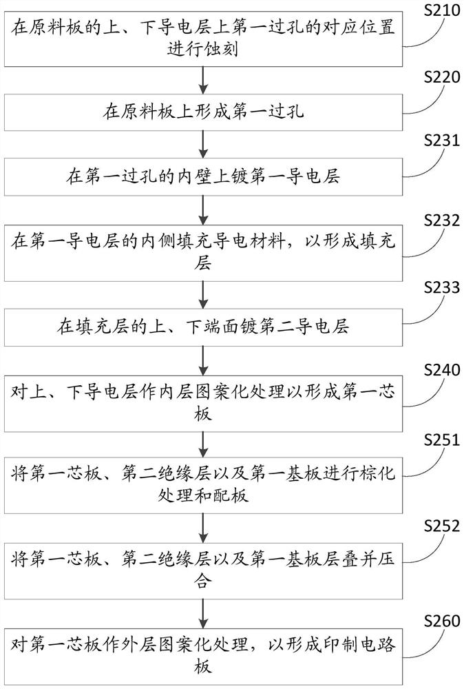
[0021] see figure 1 , the first embodiment of the method for preparing a printed circuit board of the present invention includes:
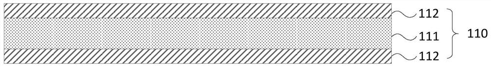
[0022] S101, forming a first via hole on the raw material board, wherein the raw material board includes a first insulating layer and upper and lower conductive layers disposed on both surfaces of the first insulating layer;
[0023] Wherein, the raw material board is a double-layer printed circuit board, and both surfaces are provided with conductive layers.
[0024] S102, performing conductive filling treatment on the first via hole to electrically connect the upper and lower conductive layers to form a first core board;
[0025] In this embodiment, the filled conductive material may be copper of the same material as the conductive layer. In other embodiments, the filled conductive material may also be other conductive metals, alloys or carbon fibers, etc., which are not limited here.
[0026] S103, laminating and pressing the first core board...
PUM
 Abstract
Description
Claims
Application Information
 - Generate Ideas
- Intellectual Property
- Life Sciences
- Materials
- Tech Scout
- Unparalleled Data Quality
- Higher Quality Content
- 60% Fewer Hallucinations
Browse by: Latest US Patents, China's latest patents, Technical Efficacy Thesaurus, Application Domain, Technology Topic, Popular Technical Reports.
© 2025 PatSnap. All rights reserved.Legal|Privacy policy|Modern Slavery Act Transparency Statement|Sitemap|About US| Contact US: help@patsnap.com