Nanoscale PN junction diode rectifier based on MnBi2Te4 single layer

A PN junction diode and diode rectifier technology is applied in the field of nano-scale electronic devices, which can solve the problems of few reports on the design of nano-devices, and achieve the effects of excellent rectification performance, adjustable size and ultra-thin structure.

Active Publication Date: 2020-11-27
HENAN NORMAL UNIV
View PDF4 Cites 0 Cited by
  • Summary
  • Abstract
  • Description
  • Claims
  • Application Information

AI Technical Summary

Problems solved by technology

However, regarding the MnBi 2 Te 4 There are few reports on the design of single-layer nanodevices

Method used


Image

  • Nanoscale PN junction diode rectifier based on MnBi2Te4 single layer
  • Nanoscale PN junction diode rectifier based on MnBi2Te4 single layer
  • Nanoscale PN junction diode rectifier based on MnBi2Te4 single layer

Examples


Embodiment

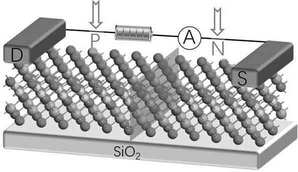
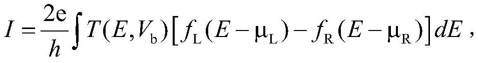
[0015] The invention is constructed by MnBi 2 Te 4 A PN junction diode device obtained by P-type doping and N-type doping at both ends of a single-layer structure of the material. The present invention uses the industry's advanced device design tool QuantumATK ( Smidstrup,et al.,QuantumATK:an integrated platform of electronic and atomic-scalemodelling tools[J].J.Phys.:Condens.Matter 32,015901(2020)) for device model design and performance measurement.

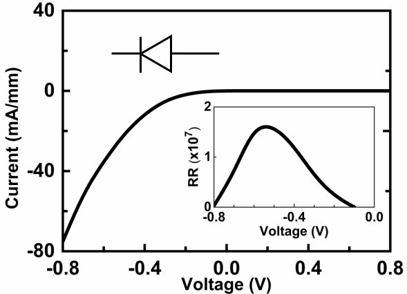
[0016] Through the measurement of its electrical properties such as current-voltage curve, it is revealed that the MnBi-based 2 Te 4 The rectification function of the single-layer nanoscale PN junction diode rectifier provides a relevant theoretical basis and model construction scheme for the further design and realization of rectifier diode nanodevices with ultra-thin structure, low power consumption, excellent performance and adjustable size.

[0017] This is based on MnBi 2 Te 4 The realization of the rectification effect of the ...


PUM


Abstract

The invention discloses a nanoscale PN junction diode rectifier based on an MnBi2Te4 single layer, and belongs to the technical field of nanoscale electronic devices. Key points of the technical scheme of the invention are as follows: the nanoscale PN junction diode rectifier based on the MnBi2Te4 single layer is composed of a single-layer structure of a MnBi2Te4 material, p-type doping is carriedout at one end of a single-layer structure of the MnBi2Te4 material, N-type doping is carried out at the other end, and a PN junction structure is formed; a drain electrode and a source electrode areapplied to the two ends of the PN junction structure respectively, and the PN junction structure is placed on a substrate such as silicon dioxide to form a diode structure; when forward bias voltageand reverse bias voltage are applied to the two ends of the diode structure respectively, the diode structure shows the rectification characteristic. The rectifier disclosed in the invention has the advantages of being ultrathin in structure, adjustable in size, remarkable in rectification effect and the like.

Description

Technical field [0001] The invention belongs to the technical field of nanoscale electronic devices, and specifically relates to a MnBi-based 2 Te 4 Single-layer nano-scale PN junction diode rectifier. Background technique [0002] In the post-Moore era, the development of silicon-based devices has encountered a major bottleneck, and it is necessary to find new materials to replace traditional silicon-based devices. Two-dimensional materials may become potential candidate materials for devices due to their unique properties in the fields of electricity and other fields. [0003] In recent years, two-dimensional monolayer materials have aroused great research interest of researchers in many fields due to their unique geometric and electronic structure, mechanical and optoelectronic properties. Such as graphene, silylene, germanene, boron nitride, transition metal disulfide, MX ene, phosphorene, tinene, boronene, etc. have been successfully prepared. A large number of studies have ...

Claims


Application Information

Patent Timeline
Patent Type & Authority Applications(China)
IPC IPC(8): H01L29/861H01L29/24B82Y40/00B82Y10/00
CPCH01L29/8611H01L29/24B82Y10/00B82Y40/00Y02B70/10
Inventor 安义鹏朱明甫武大鹏马传琦刘尚鑫康军帅焦照勇贾光瑞董晓
Owner HENAN NORMAL UNIV
Why Eureka
Try Eureka