Micro spectrum chip based on random shape unit
A miniature and spectral technology, applied in the field of spectral imaging, can solve the problems of limited broadband modulation function and limit the accuracy of spectral restoration, achieve the effects of enriching broadband modulation characteristics, realizing high-precision measurement, and improving the accuracy of spectral restoration
- Summary
- Abstract
- Description
- Claims
- Application Information
AI Technical Summary
Problems solved by technology
Method used
Image
Examples
Embodiment 1
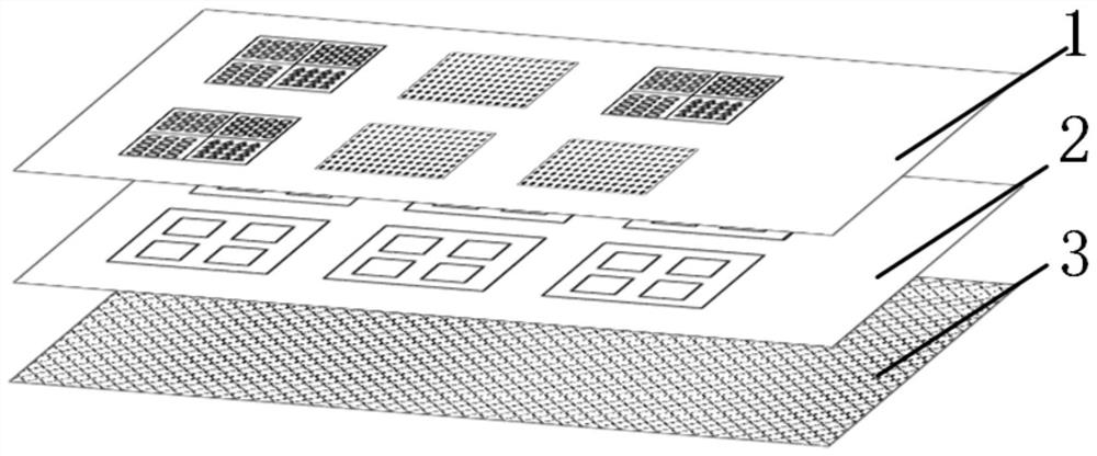
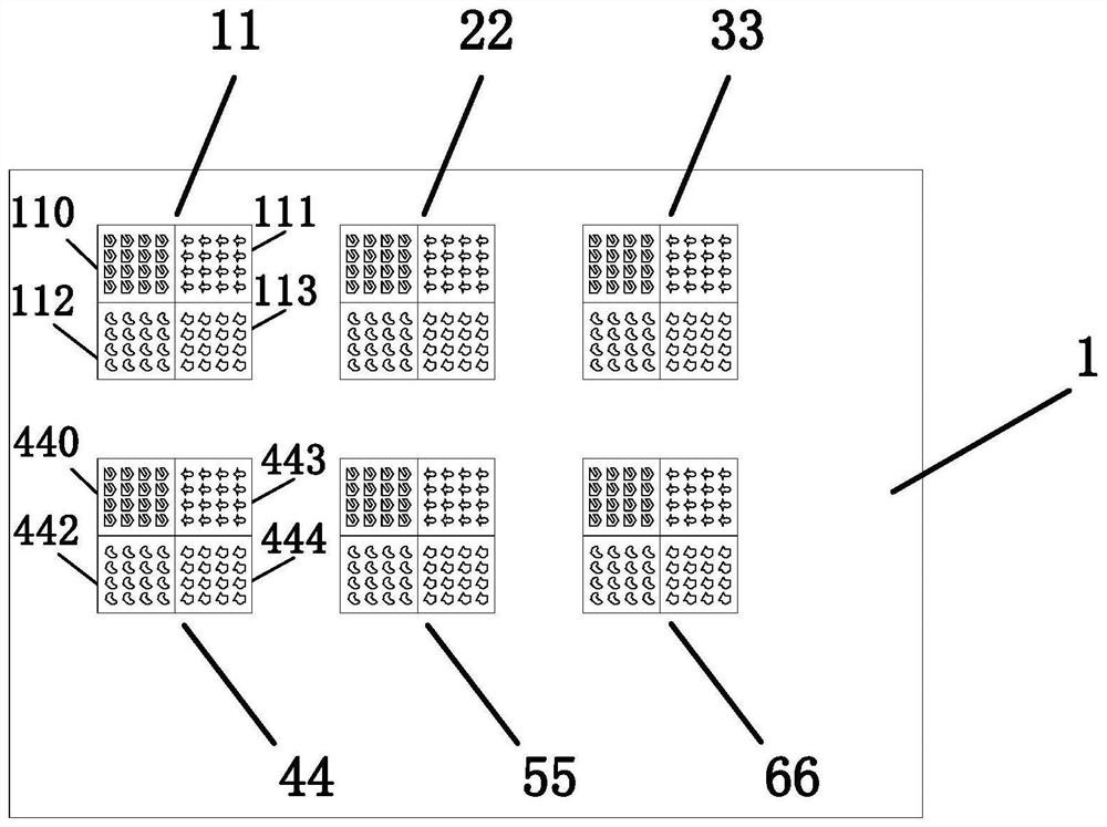
[0074] Such as Figure 13 As shown, the spectrum chip includes a light modulation layer 1 , a CIS wafer 2 and a signal processing circuit 3 . The light modulation layer 1 is directly prepared on the CIS wafer, and its lateral structure adopts the above-mentioned scheme 1, and the specific structure is as follows Figure 14 , Figure 15 As shown, the light modulation layer 1 includes multiple repeating micro-nano structural units, and each micro-nano structural unit is internally divided into 9 groups of different micro-nano structure arrays 110-118, and each group of two-dimensional gratings is periodically arranged in the same shape, The shape is an irregular shape generated randomly, and the period size of each group of micro-nano structure arrays is 20nm~50μm; each group of micro-nano structure arrays has different broad-spectrum modulation effects on incident light, and different micro-nano structure units are located at corresponding positions. The micro-nano structure ...
Embodiment 2
[0078] Such as Figure 17 As shown, the main difference between Example 2 and Example 1 lies in the lateral structure. Several micro-nano structural units constituting the light modulation layer 1 have C4 symmetry, that is, after the structure is rotated by 90°, 180° or 270°, it is different from the original structure. The structure coincides when rotated, which can make the structure have polarization-independent properties.
Embodiment 3
[0080] Such as Figure 18 As shown, the main difference from Example 1 lies in the vertical structure of the micro spectrum chip. A layer of light-transmitting medium layer 4 is added between the light modulation layer 1 and the CIS wafer 2, and the thickness of the light-transmitting medium layer 4 is 50nm~ 2 μm, the material can be silicon dioxide. If it is a process scheme of direct deposition growth, the light-transmitting medium layer can be prepared on the CIS wafer by chemical vapor deposition, sputtering, spin coating, etc., and then the light modulation layer structure can be deposited and etched on top of it. . If it is a transfer process scheme, the micro-nano structure can be prepared on the silicon dioxide first, and then the two parts are transferred to the CIS wafer as a whole. The preparation of the spectrum chip can be completed by one-time tape-out of the CMOS process, which is beneficial to reduce the failure rate of the device, improve the yield rate of t...
PUM
| Property | Measurement | Unit |
|---|---|---|
| depth | aaaaa | aaaaa |
| depth | aaaaa | aaaaa |
| thickness | aaaaa | aaaaa |
Abstract
Description
Claims
Application Information


