A kind of preparation method of ods metal thin film material
A metal thin film and ODS technology, which is applied in the field of preparation of ODS metal thin film materials, can solve problems such as coarse grains of metal blocks, and achieve the effect of simple and easy operation and uniform dispersion in the preparation process.
- Summary
- Abstract
- Description
- Claims
- Application Information
AI Technical Summary
Problems solved by technology
Method used
Image
Examples
Embodiment 1
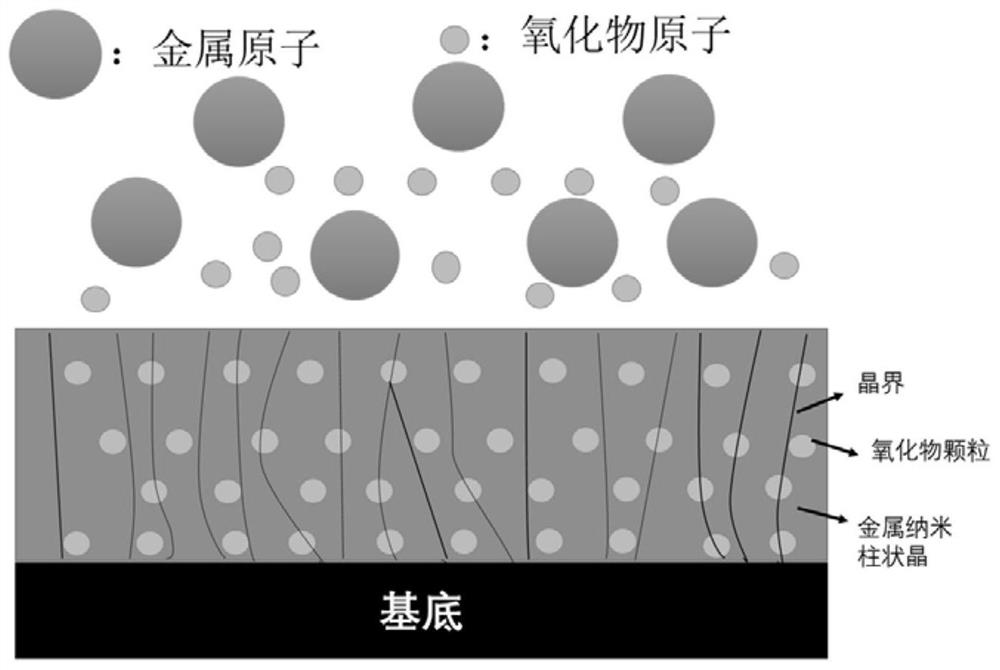
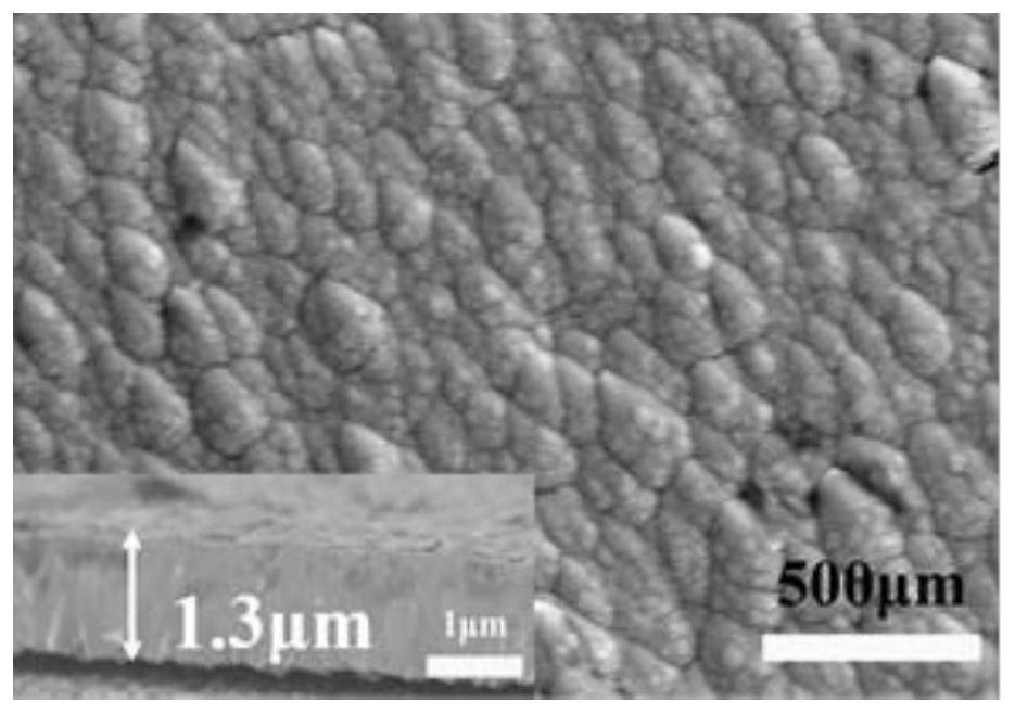
[0038] like figure 1 and figure 2 As shown, a preparation method of an ODS metal thin film material comprises the following steps:
[0039] Step 1: Take Y with an average particle size of about 50nm 2 O 3 The powder is about 2g, placed in a sleeve mold with an inner diameter of 20mm, and pressed into a disc with a diameter of 20mm and a thickness of 2mm by a tablet press. The tableting condition is 15MPa and the pressure is maintained for 5min. Heat in furnace to 1300 o C, hold for 5h, and cool with the furnace to obtain Y 2 O 3 Ceramics;
[0040] Step 2: Perform surface treatment on a 304 stainless steel metal target with a thickness of 4 mm to remove surface metal oxides and impurities to obtain a metal target; cut out two sets of symmetrical through holes from the metal target, 2 O 3 The ceramic sheet is covered with conductive adhesive on the back of the metal target, and two Ys must be added. 2 O 3 Composite target of ceramic sheet;
[0041] Step 3: The single...
Embodiment 1 and comparative example 1
[0052] The extension test of embodiment 1 and comparative example 1:
[0053] 1) First examine Y 2 O 3 The effect of the number of ceramic flakes on the oxide concentration in the film:
[0054] According to steps 1 to 4 in Example 1, other parameters are not changed, only the Y loaded on the 304 stainless steel target is changed. 2 O 3 The number of ceramic sheets is 0, 1, 2, and 4 in sequence. The Y content in the corresponding film is measured by inductively coupled plasma spectrometer (ICP) to be about 0, 0.07, 0.15, 1.02 at%, respectively. The content of Y in the film With Mosaic Y 2 O 3 The increase in slices corresponds to an increase.
[0055] 2) Next, inspect Y 2 O 3 The effect of the number of ceramic sheets on the film deposition thickness:
[0056] Under the same process conditions and sputtering conditions, the target load Y 2 O 3 The number of ceramic sheets is 0 and 2 in turn, and the film thickness is about 2.5 μm and 1.3 μm, respectively, indicating...
Embodiment 2
[0060] Compared with Example 1, the process parameters in steps 1, 3 and 4 are the same, the difference is that the composite target used in step 2 is added with four Y 2 O 3 The W target of the ceramic sheet; the surface morphology analysis and cross-sectional morphology analysis of the obtained film are shown in Figure 4(a), the film thickness is about 1 μm, and the Y in the film material is shown in Figure 4(a). 2 O 3 The distribution study of , is shown in Figure 4(b), Y 2 O 3 The particle size is about 60 nm.
PUM
| Property | Measurement | Unit |
|---|---|---|
| thickness | aaaaa | aaaaa |
| particle size | aaaaa | aaaaa |
| particle size | aaaaa | aaaaa |
Abstract
Description
Claims
Application Information


