
Method of manufacture of group iii nitride semiconductor

A technology of nitride semiconductor and manufacturing method, which is applied in the direction of semiconductor/solid-state device manufacturing, semiconductor devices, manufacturing tools, etc., can solve the problem of high cost, and achieve the effect of suppressing the deterioration of characteristics

Pending Publication Date: 2020-12-04
PANASONIC INTELLECTUAL PROPERTY MANAGEMENT CO LTD
View PDF3 Cites 0 Cited by
  • Summary
  • Abstract
  • Description
  • Claims
  • Application Information

AI Technical Summary

Problems solved by technology

[0013] SiC substrates are also expensive substrates like GaN substrates

Method used


Image

  • Method of manufacture of group iii nitride semiconductor
  • Method of manufacture of group iii nitride semiconductor
  • Method of manufacture of group iii nitride semiconductor

Examples


Embodiment approach 1

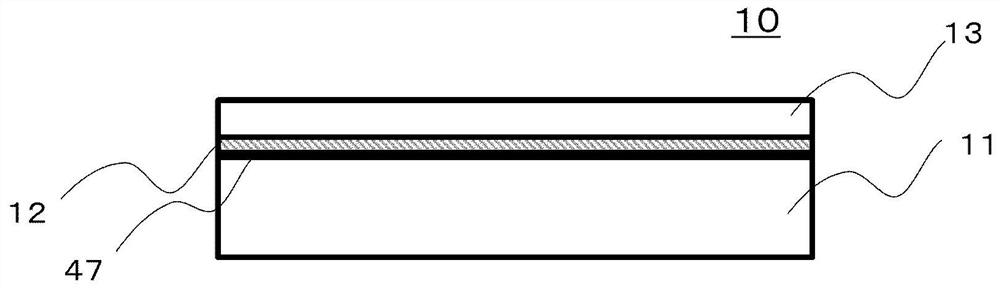
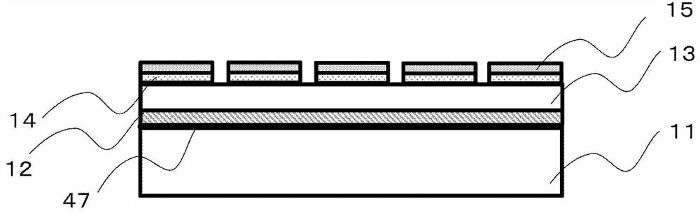
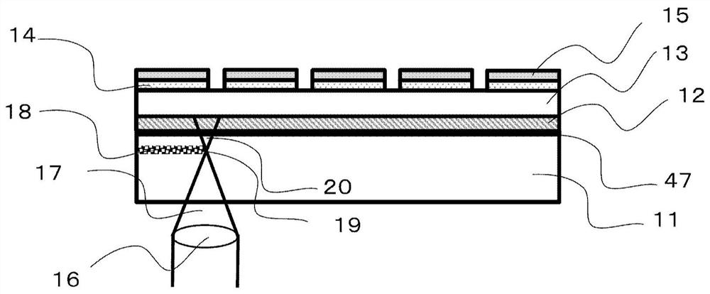
[0118] Figure 1-1 to Figure 1-4 It is a schematic cross-sectional view showing each step of the method for manufacturing a group III nitride semiconductor described in Embodiment 1.

[0119]The method for manufacturing a group III nitride semiconductor described in Embodiment Mode 1 includes the step of preparing to stack the first group III nitride layer 11 , the second group III nitride layer 12 , and the third group III nitride layer sequentially from the back side to the front side. The process ( Picture 1-1 ); a step of forming a device structure on the surface side of a group III nitride substrate ( Figure 1-2 ); and a step of dividing the III-nitride substrate by irradiating laser light from the first III-nitride layer on the back side of the III-nitride substrate ( Figure 1-3 with Figure 1-4 ). The first group III nitride layer 11 has a transmittance of 60% or more with respect to a predetermined wavelength of 400 nm to 700 nm. The second III-nitride layer is...


PUM


Abstract

The invention provides a method for manufacturing a group III nitride semiconductor, which includes: preparing a group III nitride substrate having a first group III nitride layer and a second group III nitride layer laminated in this order from a back-surface side to a front-surface side, the first group III nitride layer being a layer having a transmittance of 60% or more for a predetermined wavelength of 400 nm to 700 nm, the second group III nitride layer being a layer provided on the first group III nitride layer and containing impurity oxygen in a concentration of 1*10<-20> / cm3 or more and having a transmittance of 0.1% or less for the predetermined wavelength; forming a device structure on the front-surface side of the group III nitride substrate; and forming an internal altered layer in the first group III nitride layer by multiphoton absorption using a laser beam applied from the first group III nitride layer side on the back-surface side of the group III nitride substrate with a focal point set in front of the second group III nitride layer, and dividing the group III nitride substrate at the internal altered layer serving as a boundary.

Description

technical field [0001] The present application relates to a method of manufacturing a Group III nitride semiconductor. Background technique [0002] LEDs for white lighting with blue wavelengths, blue light (Blu-Ray) reading, laser diodes with ultraviolet to blue wavelengths used as light sources for welding processes, frequency conversion in power systems, and motor control A power device uses a single crystal Group III nitride semiconductor substrate (a GaN substrate is exemplified below) as a material. [0003] The GaN substrate generally has a thickness of 300 to 700 μm and a circular shape with a diameter of 50 to 150 mm. Generally, a GaN substrate has a transmittance of 60% or more and is transparent to visible light. [0004] On the other hand, an example of a method of fabricating a device structure from a GaN substrate is shown in Figure 5-1 to Figure 5-6 . Figure 5-1 to Figure 5-6 It is a schematic cross-sectional view showing each step in a manufacturing metho...

Claims


Application Information

Patent Timeline
IPC IPC(8): H01L21/268H01L21/302B23K26/50
CPCH01L21/268H01L21/302B23K26/50H01L21/02002H01L21/7813H01L21/187B23K26/0006B23K26/53B23K26/0624B23K2101/40B23K2103/172B23K2103/52
Inventor 岩泽绫子冈山芳央冈本贵敏
Owner PANASONIC INTELLECTUAL PROPERTY MANAGEMENT CO LTD
Features
  • Generate Ideas
  • Intellectual Property
  • Life Sciences
  • Materials
  • Tech Scout
  • Unparalleled Data Quality
  • Higher Quality Content
  • 60% Fewer Hallucinations
Learn More