Silicon carbide-based DSRD device with p-type variable doping base region and preparation method thereof

A silicon carbide-based, variable doping technology, applied in semiconductor/solid-state device manufacturing, semiconductor devices, electrical components, etc., can solve problems such as difficulty in fully utilizing silicon carbide materials, limiting DSRD device performance, and affecting carrier extraction speed , to achieve the effects of improving device reliability, shortening the pulse front, and saving costs

Active Publication Date: 2021-11-19
XIDIAN UNIV
View PDF4 Cites 0 Cited by
  • Summary
  • Abstract
  • Description
  • Claims
  • Application Information

AI Technical Summary

Problems solved by technology

[0004] However, due to the low carrier lifetime and mobility of current SiC materials and the impact of incomplete ionization effects of impurities, conventional SiC-based DSRDs locally deviate from electrical neutrality during the reverse pumping phase of pulse discharge, affecting the charge efficiency. The carrier extraction speed leads to long front time of voltage pulse, low peak value of voltage pulse, and high power consumption of the device. It is difficult to give full play to the advantages of silicon carbide materials, which limits the performance of DSRD devices.

Method used


Image

  • Silicon carbide-based DSRD device with p-type variable doping base region and preparation method thereof
  • Silicon carbide-based DSRD device with p-type variable doping base region and preparation method thereof
  • Silicon carbide-based DSRD device with p-type variable doping base region and preparation method thereof

Examples


Embodiment 1

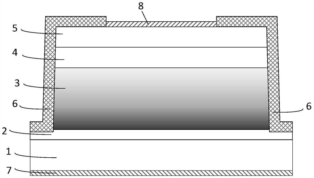
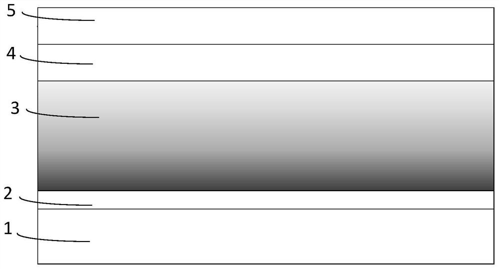
[0043] See figure 1 , figure 1It is a schematic structural diagram of a silicon carbide-based DSRD device with a P-type variable doping base region provided by an embodiment of the present invention. The SiC-based DSRD device includes substrate 1, N+ buffer zone 2, P-base region 3, P+ buffer region 4, P+ region 5, SiO 2 Passivation layer 6, cathode 7 and anode 8. The substrate 1, the N+ buffer area 2, the P-base area 3, the P+ buffer area 4 and the P+ area 5 are arranged sequentially from bottom to top.

[0044] Preferably, the substrate 1 has a thickness of 350 μm and a doping concentration of 5×10 18 cm -3 SiC material.

[0045] Preferably, the N+ buffer zone 2 is an N-type SiC material with a doping concentration of 1×10 18 cm -3 , the dopant ions are nitrogen ions.

[0046] Preferably, the P-base region 3 is a P-type SiC material with a doping concentration of 1×10 15 cm -3 to 2×10 16 cm -3 And increasing from top to bottom, the dopant ions are aluminum ions. ...

Embodiment 2

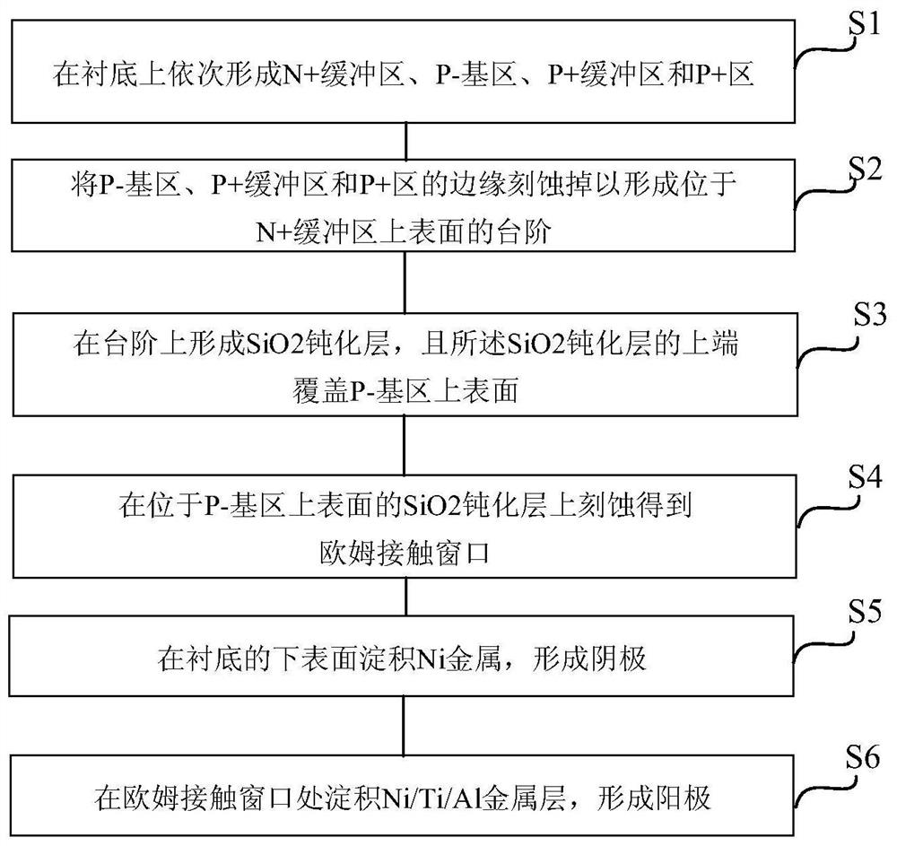
[0056] On the basis of the first embodiment, this embodiment provides a method for preparing a silicon carbide-based DSRD device with a P-type variable doping base region, which is used to prepare the silicon carbide-based DSRD device described in the first embodiment. See figure 2 , figure 2 It is a flowchart of a method for preparing a silicon carbide-based DSRD device with a P-type variable doping base region provided by an embodiment of the present invention. The preparation method includes:

[0057] S1: Form N+ buffer zone, P-base region, P+ buffer zone and P+ region sequentially on the substrate;

[0058] See Figure 3a to Figure 3f , Figure 3a to Figure 3f It is a schematic diagram of the manufacturing process of a silicon carbide-based DSRD device with a P-type variable doping base region provided by an embodiment of the present invention. Step S1 specifically includes: selecting a thickness of 350 μm and a doping concentration of 5×10 18 cm -3 RCA standard c...


PUM

PropertyMeasurementUnit
thicknessaaaaaaaaaa
thicknessaaaaaaaaaa
thicknessaaaaaaaaaa

Abstract

The invention discloses a silicon carbide-based DSRD device with a P-type variable doping base region and a preparation method thereof. The device includes a substrate, an N+ buffer region, a P-base region, a P+ buffer region, a P+ region, and a SiO 2 Passivation layer, cathode and anode, wherein, substrate, N+ buffer zone, P-base region, P+ buffer zone and P+ region are arranged sequentially from bottom to top; SiO 2 The passivation layer covers the P-base area, the P+ buffer area and the periphery of the P+ area, and the SiO 2 The upper end of the passivation layer covers part of the upper surface of the P‑base region, SiO 2 The lower end of the passivation layer covers the area on the upper surface of the N+ buffer zone that is not covered by the P-base region; the cathode is arranged on the lower surface of the substrate; the anode is arranged on the upper surface of the P+ region that is not covered by SiO 2 The area covered by the passivation layer, and the anode with SiO 2 passivation layer contacts. The device can shorten the pulse front of the silicon carbide-based DSRD, reduce device power consumption, reduce process complexity, and improve device reliability.

Description

technical field [0001] The invention belongs to the technical field of DSRD devices, and in particular relates to a silicon carbide-based DSRD device with a P-type variable doping base region and a preparation method thereof. Background technique [0002] DSRD (Drift Step Recovery Diodes, Drift Step Fast Recovery Diodes) is a semiconductor circuit breaker diode, which has the characteristics of high efficiency, high reliability, long continuous working time and small size, and is usually used as a key device in UWB (Ultra Wide Band, ultra-wideband) pulse signal source. [0003] Due to the theoretical limit of silicon materials, silicon-based DSRDs have been unable to meet the requirements of most pulse systems of several kilovolts or even tens of kilovolts. Silicon carbide materials have higher bandgap width, saturation drift velocity, thermal conductivity, critical breakdown electric field and radiation resistance than silicon materials, making the performance of silicon c...

Claims


Application Information

Patent Timeline
Patent Type & Authority Patents(China)
IPC IPC(8): H01L29/868H01L21/329H01L29/06H01L29/16
CPCH01L29/0684H01L29/1608H01L29/6606H01L29/868
Inventor 汤晓燕周瑜宋庆文袁昊何艳静张玉明
Owner XIDIAN UNIV
Why Eureka
Try Eureka