X-ray detector based on field effect transistor structure and preparation method thereof

A field effect transistor and X-ray technology is applied in the field of X-ray detectors based on field effect transistor structures and their preparation, and can solve the problems of low sensitivity, bulkiness, complicated material growth and preparation process, etc.

Inactive Publication Date: 2020-12-08
深圳市中科瑞和企业管理服务有限公司
View PDF6 Cites 2 Cited by
  • Summary
  • Abstract
  • Description
  • Claims
  • Application Information

AI Technical Summary

Problems solved by technology

[0003] In order to overcome the deficiencies of the prior art, the technical problem to be solved by the present invention is to provide a variety of new high-performance field-effect transistor X-ray detectors with heterojunctions composed of channel semiconductors and X-ray photoconductive materials,...

Method used


Image

  • X-ray detector based on field effect transistor structure and preparation method thereof
  • X-ray detector based on field effect transistor structure and preparation method thereof
  • X-ray detector based on field effect transistor structure and preparation method thereof

Examples


Embodiment 1

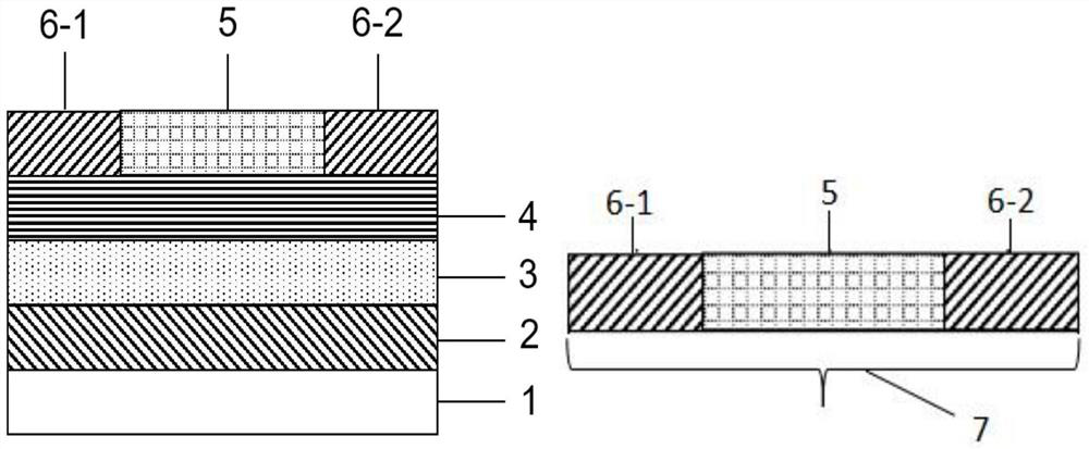
[0081] Such as Figure 1a and Figure 1b It is a schematic diagram of the first device structure of the X-ray detector of the present invention, such as Figure 1a , including a substrate 1, located at the bottom of the X-ray detector; a gate electrode 2, the lower surface of the gate electrode 2 is made on the upper surface of the substrate 1; a gate dielectric layer 3, used for insulation, the The lower surface of the gate dielectric layer 3 is made on the upper surface of the gate electrode 2; the semiconductor channel layer 4 is used to transmit charges to generate channel current, and the lower surface of the semiconductor channel layer 4 is made on the said gate electrode 2. The upper surface of the gate dielectric layer 3; the X-ray layer 7 includes an X-ray absorbing layer 5, a source electrode 6-1 and a drain electrode 6-2, and the lower surface of the X-ray layer 7 is made on the semiconductor The upper surface of the channel layer 4, wherein the lower surface of the...

Embodiment 2

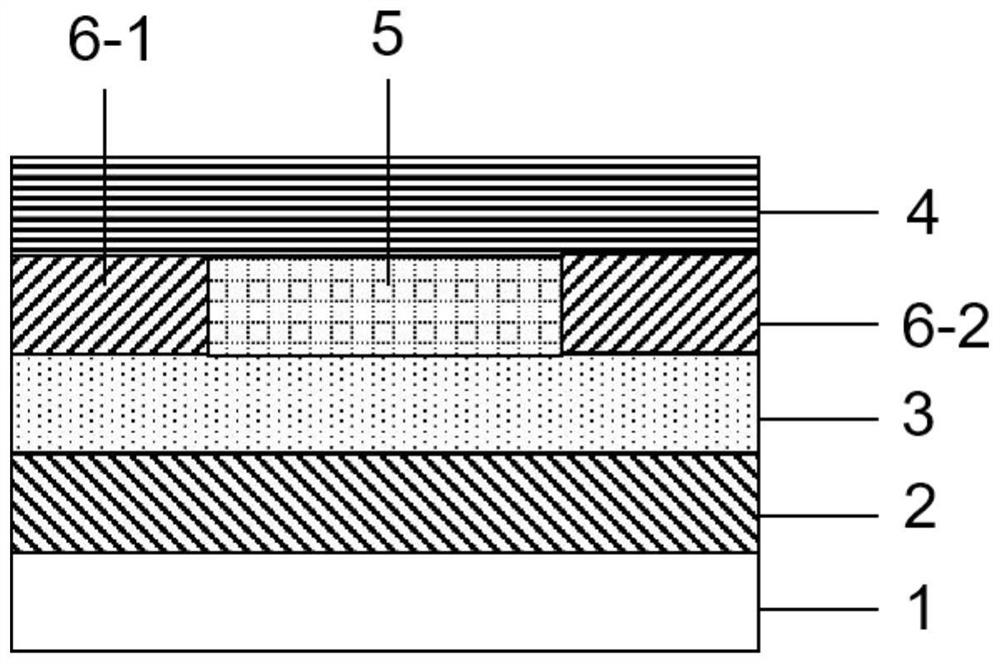
[0085] Such as Figure 2a and Figure 2b It is a schematic diagram of the second device structure of the X-ray detector of the present invention, such as Figure 2a , including a substrate 1, located at the bottom of the X-ray detector; a gate electrode 2, the lower surface of the gate electrode 2 is made on the upper surface of the substrate 1; a gate dielectric layer 3, used for insulation, the The lower surface of the gate dielectric layer 3 is made on the upper surface of the gate electrode 2; the semiconductor channel layer 4 is used to transmit charges to generate channel current, and the lower surface of the semiconductor channel layer 4 is made on the said gate electrode 2. The upper surface of the gate dielectric layer 3; the X-ray absorbing layer 5, the lower surface of the X-ray absorbing layer 5 is made on the upper surface of the semiconductor channel layer 4; the source electrode 6-1 and the drain electrode 6-2, the lower surface of the source electrode 6-1 and...

Embodiment 3

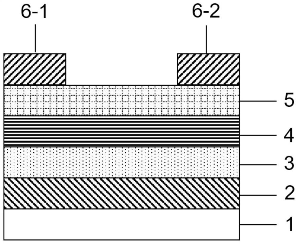
[0089] Such as Figure 3a and Figure 3b It is a schematic diagram of the third device structure of the X-ray detector of the present invention, such as Figure 3a , including a substrate 1, located at the bottom of the X-ray detector; a gate electrode 2, the lower surface of the gate electrode 2 is made on the upper surface of the substrate 1; a gate dielectric layer 3, used for insulation, the The lower surface of the gate dielectric layer 3 is made on the upper surface of the gate electrode 2; the semiconductor layer 8 includes a semiconductor channel layer 4, a source electrode 6-1 and a drain electrode 6-2, and the semiconductor layer 8 The lower surface of layer 8 is formed on the upper surface of the gate dielectric layer 3, wherein the lower surface of the semiconductor channel layer 4 is formed in the middle of the upper surface of the gate dielectric layer 3, covering all A part of the upper surface of the gate dielectric layer 3, the source electrode 6-1 and the d...


PUM


Abstract

The invention discloses an X-ray detector based on a field effect transistor structure and a preparation method of the X-ray detector, and the X-ray detector comprises an X-ray absorption layer capable of absorbing X-rays, a semiconductor channel layer, a gate electrode, a gate dielectric layer, a source electrode, a drain electrode and a substrate. After the X-rays are irradiated to the X-ray absorption layer of the X-ray detector, electron-hole pairs are generated in the X-ray absorbing layer, electrons or holes generated by X-ray irradiation can be transferred from the X-ray absorption layer to the semiconductor channel layer, and the electrons or holes flow between the source electrode and the drain electrode to generate current. Compared with a traditional X-ray detector based on a diode, a photoelectric transistor combines the advantages of a transistor and a conventional photoconductive device, obtains efficient charge transfer by means of a heterojunction structure, generates ahuge gain amplification effect by means of efficient transmission of carriers in a semiconductor channel, and therefore, the high-performance X-ray detector with ultrahigh sensitivity and ultralow detection limit is obtained.

Description

technical field [0001] The invention belongs to the field of X-ray detectors, in particular to an X-ray detector based on a field-effect transistor structure and a preparation method thereof. Background technique [0002] X-ray detectors have important application value in the fields of medical diagnosis, scientific research, industrial non-destructive testing and national defense security. X-ray detectors are mainly based on two photoelectric conversion mechanisms: one is the direct X-ray detector, which directly converts the X-ray signal into an electrical signal through a photosensitive semiconductor material; the other is the indirect X-ray detector, which first passes through the scintillation The body converts X-rays into visible light, and then completes the conversion of optical signals into electrical signals through visible light detectors. At present, X-ray photodetectors based on these two photoelectric conversion mechanisms have been commercialized, but there a...

Claims


Application Information

Patent Timeline
IPC IPC(8): H01L31/119H01L31/18G01T1/24
CPCH01L31/119H01L31/18G01T1/241Y02P70/50
Inventor 高源鸿李建华
Owner 深圳市中科瑞和企业管理服务有限公司
Why Eureka
Try Eureka