Active driving circuit and method of MOSFET

A technology of source driving and driving resistance, which is applied in the field of power electronics, can solve the problems of poor suppression effect, large switching loss, and long switching time, and achieve the effects of reducing switching loss and cost, suppressing current overshoot, and shortening switching time

Pending Publication Date: 2020-12-08
CHINA ELECTRIC POWER RES INST +1
View PDF0 Cites 1 Cited by
  • Summary
  • Abstract
  • Description
  • Claims
  • Application Information

AI Technical Summary

Problems solved by technology

[0005] In order to overcome the shortcomings of poor suppression effect, high cost, long switching time and large switching loss in the above-mentioned prior art, the present invention provides an active drive circuit for MOSFET, including a push-pull module, a resistance module and a pulse generation module;

Method used


Image

  • Active driving circuit and method of MOSFET
  • Active driving circuit and method of MOSFET
  • Active driving circuit and method of MOSFET

Examples


Embodiment 1

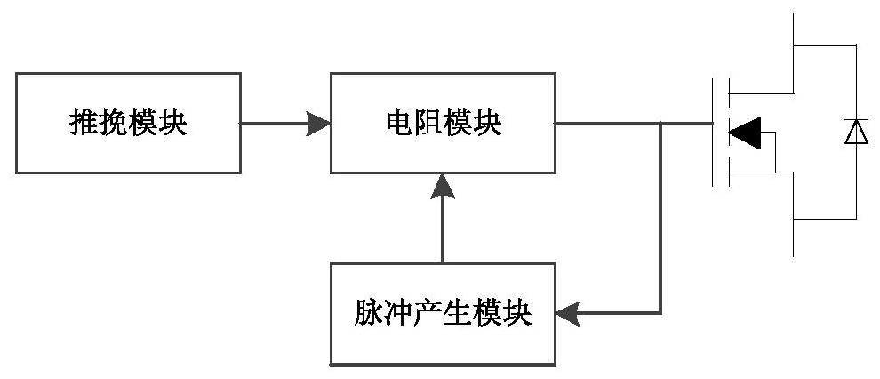
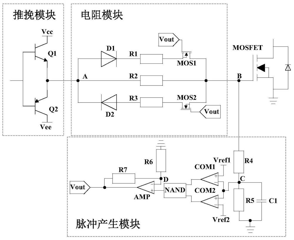
[0051] Embodiment 1 of the present invention provides an active drive circuit for MOSFET, such as figure 1 As shown, including push-pull module, resistance module and pulse generation module;

[0052] The push-pull module is connected to the gate of the driven MOSFET through the resistance module, one end of the pulse generating module is connected to the gate of the driven MOSFET, and the other end is connected to the resistance module;

[0053] Based on the driving voltage of the driven MOSFET generated by the push-pull module and the pulse signal generated by the pulse generating module based on the collected gate-source voltage of the driven MOSFET, a variable driving resistance is provided for the driven MOSFET.

[0054] The pulse generating module includes a sampling circuit, a pulse generating circuit and an amplifying circuit;

[0055] One end of the sampling circuit is connected to the gate of the driven MOSFET, and the other end is connected to the input end of the ...

Embodiment 2

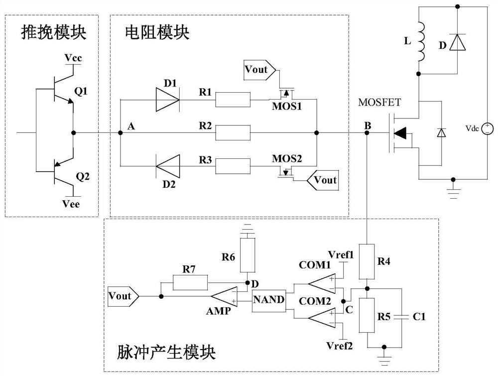
[0072] Embodiment 2 of the present invention provides an active driving method for MOSFET, such as Image 6 shown, including:

[0073] S101: the push-pull module generates the driving voltage of the driven MOSFET;

[0074] S102: the pulse generating module collects the gate-source voltage of the driven MOSFET, and generates a pulse signal based on the gate-source voltage;

[0075] S103: the resistance module provides variable driving resistance for the driven MOSFET based on the driving voltage and the pulse signal.

[0076] In the above S103, the resistance module provides a variable driving resistance for the driven MOSFET based on the driving voltage and the pulse signal, which is specifically divided into two cases: MOSFET turn-on process and turn-off process.

[0077] During the MOSFET turn-on process, the resistance module provides variable driving resistance for the driven MOSFET based on the driving voltage and pulse signal, including:

[0078] The sampling circuit ...


PUM


Abstract

The invention provides an active driving circuit and method of an MOSFET. The active driving circuit comprises a push-pull module, a resistor module and a pulse generation module. The push-pull moduleis connected with the grid electrode of the driven MOSFET through the resistor module, one end of the pulse generation module is connected with the grid electrode of the driven MOSFET, and the otherend of the pulse generation module is connected with the resistor module. The variable driving resistance is provided for the driven MOSFET based on the driving voltage of the driven MOSFET generatedby the push-pull module and the pulse signal generated by the pulse generation module based on the acquired gate-source voltage of the driven MOSFET. According to the circuit, a driving resistor doesnot need to be added, and the variable driving resistor is provided through the resistor module, so that the switching time of the MOSFET is shortened, the switching loss and cost are reduced, and thesuppression effect is good; the circuit is simple in structure, and current and voltage overshoot and oscillation in the switching process of the device can be effectively suppressed on the basis ofsacrificing relatively small MOSFET switching loss.

Description

technical field [0001] The invention relates to the technical field of power electronics, in particular to an active drive circuit and method for a MOSFET. Background technique [0002] Metal-oxide-semiconductor field-effect transistor MOSFET is a semiconductor device widely used in analog circuits and digital circuits. With its advantages of fast switching speed, low power consumption, stable performance and strong radiation resistance, it is gradually replacing triodes and is widely used. In photovoltaic inverters, electric vehicles and wind power generation and other fields. [0003] Compared with Si (silicon) materials, SiC (silicon carbide) materials have the advantages of higher critical breakdown field strength, higher forbidden band width, higher saturated carrier mobility and higher thermal conductivity. Therefore, compared with Si MOSFET, SiC MOSFET has higher breakdown voltage, lower on-resistance, faster switching speed and higher operating temperature. However...

Claims


Application Information

Patent Timeline
Patent Type & Authority Applications(China)
IPC IPC(8): H03K17/567
CPCH03K17/567
Inventor 余豪杰杨波李官军陶以彬殷实李浩源鄢盛驰庄俊
Owner CHINA ELECTRIC POWER RES INST
Why Eureka
Try Eureka