Alpha-indium selenide two-dimensional photoelectric detector based on transparent electrode

A photodetector and transparent electrode technology, applied in the field of photodetectors, can solve the problems of small spectral response range, non-response, limited application of related devices, etc., to increase the photoelectric response range, reduce the size of the device, and increase the photoelectric responsivity. Effect

Pending Publication Date: 2020-12-11
XI AN JIAOTONG UNIV
View PDF8 Cites 1 Cited by
  • Summary
  • Abstract
  • Description
  • Claims
  • Application Information

AI Technical Summary

Problems solved by technology

However, the single energy band structure of traditional semiconductor materials leads to a small spectral response range, which in turn causes the problem of low spectral response or even no response in some bands, which limits the application of related devices in the field of photoelectric detection.
[0004] Metal electrodes are mostly used for photodetector electrodes. For thicker metal electrodes, the transmittance is low, which affects the absorption of incident light by the photoelectric functional layer of the device.

Method used


Image

  • Alpha-indium selenide two-dimensional photoelectric detector based on transparent electrode
  • Alpha-indium selenide two-dimensional photoelectric detector based on transparent electrode
  • Alpha-indium selenide two-dimensional photoelectric detector based on transparent electrode

Examples


Embodiment Construction

[0022] The present invention is described in further detail below in conjunction with accompanying drawing:

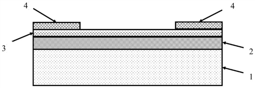
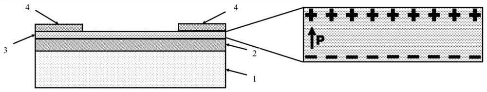
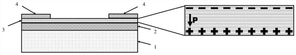
[0023] refer to figure 1 , figure 2 and image 3 The transparent electrode-based alpha-indium selenide two-dimensional photodetector according to the present invention comprises an alpha-indium selenide two-dimensional ferroelectric semiconductor layer 3, a hafnium dioxide dielectric layer 2 and a doped A silicon substrate 1, wherein a transparent electrode 4 is arranged on the α-InSe two-dimensional ferroelectric semiconductor layer 3 .

[0024] The doped silicon substrate 1 is an n-doped silicon substrate or a p-doped silicon substrate; the thickness of the hafnium dioxide dielectric layer 2 is 10-15 mm; the thickness of the α-indium selenide two-dimensional ferroelectric semiconductor layer 3 is 50-100mm; the thickness of the transparent electrode 4 is less than 100nm.

[0025] The transparent electrode 4 is a graphene film, an indium tin oxide semiconductor tr...


PUM

PropertyMeasurementUnit
thicknessaaaaaaaaaa
thicknessaaaaaaaaaa
thicknessaaaaaaaaaa

Abstract

The invention discloses an alpha-indium selenide two-dimensional photoelectric detector based on a transparent electrode, which comprises an alpha indium selenide two-dimensional ferroelectric semiconductor layer, a hafnium oxide dielectric layer and a doped silicon substrate which are sequentially distributed from top to bottom, the alpha-indium selenide two-dimensional ferroelectric semiconductor layer is provided with the transparent electrode, and the detector is small in size and low in cost. Photoelectric responsivity is high.

Description

technical field [0001] The invention relates to a photodetector that can be used in integrated circuits, in particular to a two-dimensional alpha-indium selenide photodetector based on transparent electrodes. Background technique [0002] With the development of silicon-based semiconductor integrated circuits, the size of nano-semiconductor devices continues to shrink, and the emergence of nano-scale devices has greatly promoted the development of the electronic information industry. However, the reduction in device size is also accompanied by an increase in power consumption. At the same time, due to the limitations of production equipment and quantum effects, the development of silicon-based semiconductor devices has encountered a bottleneck. The road to the further development of integrated devices In addition to making more efforts in terms of device size and power consumption, the functions of integrated devices are also developing in the direction of realizing multiple...

Claims


Application Information

Patent Timeline
Patent Type & Authority Applications(China)
IPC IPC(8): H01L31/101H01L31/0216H01L31/0392
CPCH01L31/101H01L31/02161H01L31/0392H01L31/03921
Inventor 牛刚孙延笑赵金燕史鹏任巍
Owner XI AN JIAOTONG UNIV
Why Eureka
Try Eureka