SSD laminated layout structure and design method and device

A technology of structural design and layout, applied in CAD circuit design, computer-aided design, calculation, etc., can solve the problems of compressing product board layout and wiring space, unable to ensure sufficient test board verification, unable to truly restore product board design, etc. , to shorten the development cycle, the design principle is reliable, and the substantive characteristics are highlighted.

Active Publication Date: 2020-12-15
INSPUR SUZHOU INTELLIGENT TECH CO LTD
View PDF2 Cites 0 Cited by
  • Summary
  • Abstract
  • Description
  • Claims
  • Application Information

AI Technical Summary

Problems solved by technology

The traditional method is to distribute these traces to other layers of the product board, and then delete the added parts and traces when the product board is produced. This will compress the layout and wiring space of the product board, and cannot truly restore the design of the product board. Thereby it is not possible to guarantee that the test boards are adequately verified

Method used


Image

  • SSD laminated layout structure and design method and device
  • SSD laminated layout structure and design method and device
  • SSD laminated layout structure and design method and device

Examples


Embodiment 1

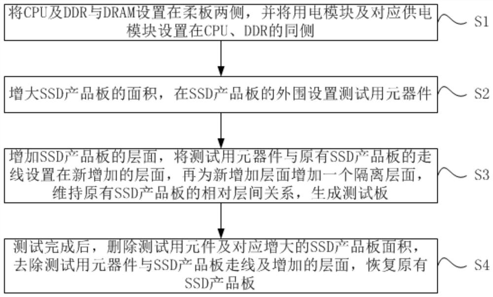
[0075] Such as figure 1 As shown, the present invention provides a method for designing a SSD stack layout structure, comprising the following steps:

[0076] S1. Set the CPU, DDR and DRAM on both sides of the flexible board, and set the power module and the corresponding power supply module on the same side of the CPU and DDR;

[0077] S2. increase the area of ​​the SSD product board, and set the components for testing on the periphery of the SSD product board;

[0078] S3. Increase the level of the SSD product board, set the wiring between the test components and the original SSD product board on the newly added layer, and then add an isolation layer for the newly added layer to maintain the relative interlayer of the original SSD product board relationship, generate a test board;

[0079] S4. After the test is completed, delete the test components and correspondingly increased SSD product board area, remove the test components and SSD product board wiring and the increase...

Embodiment 2

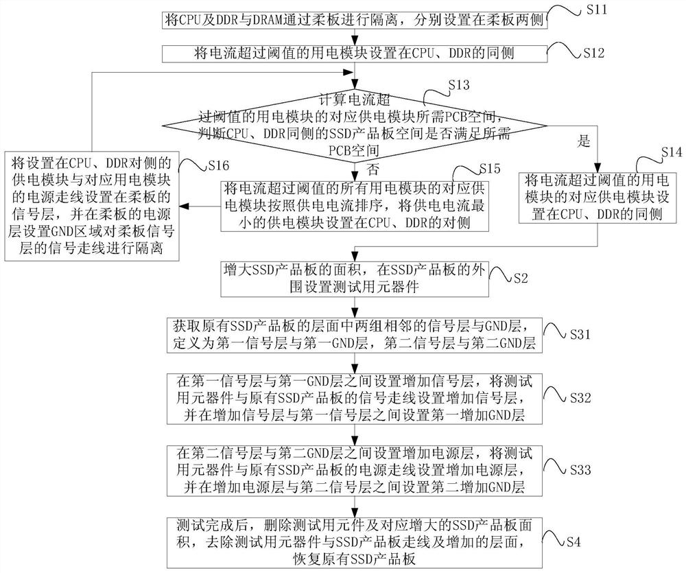
[0081] Such as figure 2 As shown, the present invention provides a method for designing a SSD stack layout structure, comprising the following steps:

[0082] S1. Set the CPU, DDR, and DRAM on both sides of the flexible board, and set the power module and the corresponding power supply module on the same side of the CPU and DDR; the specific steps are as follows:

[0083] S11. Isolate the CPU, DDR and DRAM through the flexible board, and set them on both sides of the flexible board;

[0084] S12. Set the power consumption module whose current exceeds the threshold on the same side of the CPU and DDR;

[0085] S13. Calculate the PCB space required by the corresponding power supply module of the power consumption module whose current exceeds the threshold, and judge whether the SSD product board space on the same side as the CPU and DDR meets the required PCB space;

[0086] If yes, go to step S14;

[0087] If not, go to step S15;

[0088] S14. Set the corresponding power s...

Embodiment 3

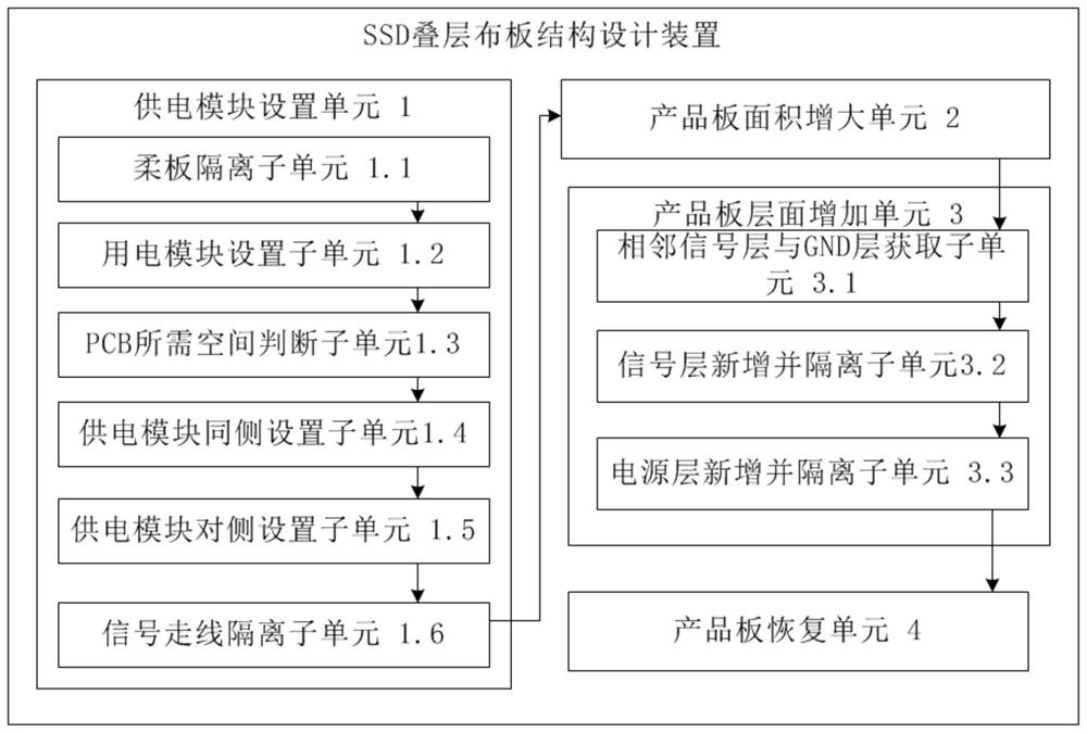
[0101] The present invention provides an SSD stacked layout structure, including an original wiring layer and a newly added wiring layer;

[0102] The original wiring layer includes the SSD product board area and the test area; the test area is set on the periphery of the SSD product board area, and the test area is provided with test components;

[0103] The SSD product board area includes a flex board, and the flex board divides the SSD product board area into a first area and a second area, the first area is provided with DRAM, and the second area is provided with CPU, DRAM, power module and first power supply module; The first power supply module is connected to the CPU, the DRAM and the power consumption module;

[0104] The newly added wiring layer includes a functional layer and an isolation layer, and the functional layer and the isolation layer are arranged adjacent to each other;

[0105] The traces of the test components and the components in the SSD product board ...


PUM


Abstract

The invention provides an SSD laminated layout structure and a design method and device, and the method comprises the following steps: S1, enabling a CPU, a DDR and a DRAM to be disposed at two sidesof a flexible board, and enabling a power utilization module and a corresponding power supply module to be disposed at the same side of the CPU and the DDR; s2, increasing the area of the SSD productboard, and setting test components on the periphery of the SSD product board; s3, increasing the layers of the SSD product board, setting the wiring of the test component and the original SSD productboard at the newly increased layer, adding an isolation layer for the newly increased layer, maintaining the relative interlayer relationship of the original SSD product board, and generating a test board; and S4, after the test is completed, deleting the test element and the correspondingly increased SSD product board area, removing the test element and SSD product board wiring and the increasedlayer surface, and recovering the original SSD product board.

Description

technical field [0001] The invention belongs to the technical field of SSD layout, and in particular relates to an SSD laminated layout structure, design method and device. Background technique [0002] PCB is the abbreviation of Printed Circuit Board, printed circuit board. [0003] SSD is the abbreviation of Solid State Drive, solid state drive. [0004] DRAM is the abbreviation of Dynamic RAM, dynamic random access memory. [0005] DDR is the abbreviation of Double Data Rate, double rate synchronous dynamic random access memory. [0006] In the storage project, the update speed of SSD products is getting faster and faster, and the corresponding main control chip must also be upgraded accordingly. In order to seize the opportunity in the storage market faster, we usually do the A batch of test boards, after the pre-research is completed, the plan will be adjusted according to the test situation of the test boards, and then the product board will be designed. In the pre...

Claims


Application Information

Patent Timeline
Patent Type & Authority Applications(China)
IPC IPC(8): G06F30/392H05K3/46G06F115/12
CPCG06F30/392H05K3/4614G06F2115/12
Inventor 郭丹萍
Owner INSPUR SUZHOU INTELLIGENT TECH CO LTD
Why Eureka
Try Eureka