Self-aligned superconducting nanowire single-photon detection device and packaging method thereof

A superconducting nanowire and single-photon detection technology, which is applied in the field of optical detection, can solve the problems of time-consuming, laborious and cumbersome alignment process, and the detection sensitivity decrease of superconducting nanowire single-photon detection chip, so as to achieve fast alignment and simplify alignment. quasi-process effect

Inactive Publication Date: 2020-12-18
SHANGHAI INST OF MICROSYSTEM & INFORMATION TECH CHINESE ACAD OF SCI
View PDF5 Cites 2 Cited by
  • Summary
  • Abstract
  • Description
  • Claims
  • Application Information

AI Technical Summary

Problems solved by technology

During the detection process, when the light detection surface of the superconducting nanowire single-photon detection chip is not aligned with the fiber head, all the light emitted from the fiber head will not be incident on the detection surface of the superconducting nanowire single-photon detection chip, which will lead to super The detection sensitivity of the conductive nanowire single photon detection chip decreases, which affects the detection results of the superconducting nanowire single photon detection chip
[0005] In the prior art, the optical fiber head is usually manually aligned with the superconducting nanowire single-photon detection chip. It is extremely inconvenient to detect the linear single photon detection chip

Method used


Image

  • Self-aligned superconducting nanowire single-photon detection device and packaging method thereof
  • Self-aligned superconducting nanowire single-photon detection device and packaging method thereof
  • Self-aligned superconducting nanowire single-photon detection device and packaging method thereof

Examples


Embodiment Construction

[0058] Embodiments of the present invention are described below through specific examples, and those skilled in the art can easily understand other advantages and effects of the present invention from the content disclosed in this specification. The present invention can also be implemented or applied through other different specific implementation modes, and various modifications or changes can be made to the details in this specification based on different viewpoints and applications without departing from the spirit of the present invention.

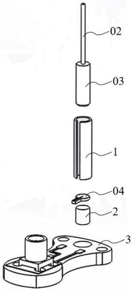
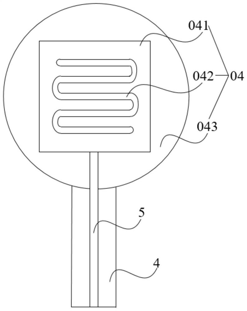
[0059]The superconducting nanowire single-photon detection chip is used for generating electrical signals under the excitation of photons incident on the detection surface of the superconducting nanowire single-photon detection chip. Superconducting nanowire single-photon detection chips can be used to detect photons. When using a superconducting nanowire single-photon detection chip to detect photons, an optical fiber is usually used...


PUM

PropertyMeasurementUnit
thicknessaaaaaaaaaa
widthaaaaaaaaaa

Abstract

The invention belongs to the technical field of optical detection, and relates to a self-aligned superconducting nanowire single-photon detection device and a packaging method thereof. The self-aligned superconducting nanowire single-photon detection device comprises a superconducting nanowire single-photon detection chip; a chip fixing member, wherein the chip fixing member is provided with a packaging hole; wherein the superconducting nanowire single-photon detection chip is installed in the packaging hole, the optical fiber head is inserted into the packaging hole and is opposite to the detection surface of the superconducting nanowire single-photon detection chip, and the shape of the cross section of the optical fiber head is the same as that of the cross section of the packaging hole, and photons emitted by the optical fiber head are incident to the detection surface. According to the self-aligned superconducting nanowire single-photon detection device, the packaging hole is formed in the chip fixing piece, the superconducting nanowire single-photon detection chip is installed in the packaging hole, the optical fiber head used for emitting light is inserted into the packaginghole, and rapid alignment of the optical fiber head and the superconducting nanowire single-photon detection chip can be achieved.

Description

technical field [0001] The invention belongs to the technical field of light detection, and relates to a self-aligned superconducting nanowire single-photon detection device and a packaging method thereof. Background technique [0002] Superconducting nanowire single-photon detection chip, or SNSPD, is a type of single-photon detection chip based on the principle of superconductivity. Compared with traditional semiconductor single-photon detectors (avalanche photodiodes and photomultiplier tubes), the advantage of SNSPD is the response speed Fast, low dark count, small time jitter, high count rate and wide response frequency band, etc. This makes it have a wide range of application prospects in quantum communication, laser radar and other fields. [0003] The superconducting nanowire single-photon detection chip is in the low-temperature superconducting state, and under the excitation of photons, it will generate a local quench, that is, a resistance region, and will form a...

Claims


Application Information

Patent Timeline
Patent Type & Authority Applications(China)
IPC IPC(8): G01J1/44G01J1/04B82Y15/00B82Y40/00
CPCB82Y15/00B82Y40/00G01J1/04G01J1/44G01J2001/442
Inventor 李浩耿荣鑫尤立星王镇谢晓明
Owner SHANGHAI INST OF MICROSYSTEM & INFORMATION TECH CHINESE ACAD OF SCI
Why Eureka
Try Eureka