Transparent Ga2O3 p-i-n heterostructure solar-blind ultraviolet light detector and preparation method thereof
A p-i-n, heterostructure technology, applied in the field of inorganic non-metallic material electronic device manufacturing process, can solve the problems of fragile photomultiplier tubes, large bias voltage, bulky and other problems, and achieves increased effective working area, large forbidden band Width, excellent performance
- Summary
- Abstract
- Description
- Claims
- Application Information
AI Technical Summary
Problems solved by technology
Method used
Image
Examples
Embodiment 1
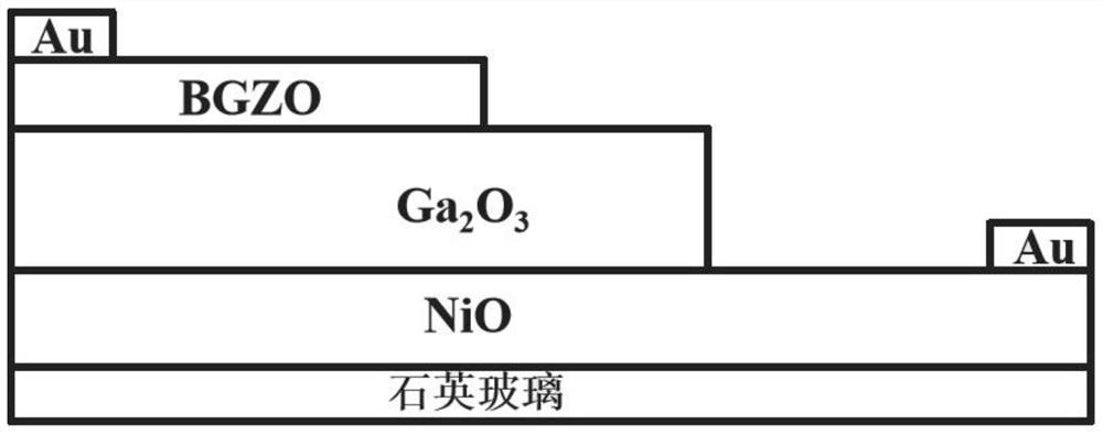
[0027] In this example, see figure 1 , a transparent Ga 2 o 3 The p-i-n heterostructure sun-blind ultraviolet detector consists of substrate, p-type NiO thin film, i-layer Ga 2 o 3 Thin film, n-type boron, gallium co-doped zinc oxide (BGZO) thin film and Au electrode are stacked and assembled to form a transparent thin film detector structure, and the substrate is made of quartz glass. Transparent Ga 2 o 3 The p-i-n heterostructure sun-blind ultraviolet light detector adopts the p-i-n structure to increase the width of the depletion region, which improves the responsivity of the device. Above-mentioned NiO film thickness is 200nm; above-mentioned Ga 2 o 3 The thickness of the film is 250nm; the thickness of the zinc oxide film co-doped with boron and gallium is 100nm; the thickness of the above gold electrode is 70nm.
[0028] A kind of transparent Ga of this embodiment 2 o 3 The structure of the p-i-n heterostructure sun-blind ultraviolet photodetector consists of s...
Embodiment 2
[0043] This embodiment is basically the same as Embodiment 1, especially in that:
[0044] In this example, a transparent Ga 2 o 3 The p-i-n heterostructure sun-blind ultraviolet detector consists of substrate, p-type NiO thin film, i-layer Ga 2 o 3 Thin film, n-type boron, gallium co-doped zinc oxide (BGZO) thin film and Au electrode are stacked and assembled to form a transparent thin film detector structure, and the substrate is made of quartz glass. Transparent Ga 2 o 3 The p-i-n heterostructure sun-blind ultraviolet light detector adopts the p-i-n structure to increase the width of the depletion region, which improves the responsivity of the device. Above-mentioned NiO film thickness is 200nm; above-mentioned Ga 2 o 3 The thickness of the film is 350nm; the thickness of the zinc oxide film co-doped with boron and gallium is 100nm; the thickness of the above gold electrode is 70nm.
[0045] A kind of transparent Ga of this embodiment 2 o 3 The structure of the p-...
PUM
| Property | Measurement | Unit |
|---|---|---|
| thickness | aaaaa | aaaaa |
| thickness | aaaaa | aaaaa |
| thickness | aaaaa | aaaaa |
Abstract
Description
Claims
Application Information
