Device and method for measuring surface contours of micro-nano devices based on optical frequency comb

A device surface and measurement device technology, applied in the direction of measurement devices, optical devices, instruments, etc., can solve the problems that cannot meet the measurement requirements of micro-nano devices, cannot cope with the characteristic size of micro-nano devices, and take a long time to measure. The effect of flux measurement requirements, fast measurement speed, and reduced requirements

Active Publication Date: 2022-04-22
INST OF MICROELECTRONICS CHINESE ACAD OF SCI
View PDF7 Cites 0 Cited by
  • Summary
  • Abstract
  • Description
  • Claims
  • Application Information

AI Technical Summary

Problems solved by technology

[0005] (1) The traditional probe-type measurement method is to achieve contour measurement by point-by-point scanning. White light interferometry requires high-precision focusing, and optical comb array measurement requires scanning repetition frequency. The above methods take a long time to measure and cannot meet the requirements of micro High-throughput measurement requirements on nano-device production lines
[0006] (2) The lateral resolution of the white light interferometry method is limited by the optical diffraction limit and the numerical aperture of the objective lens, and the lateral resolution of the area array measurement method is limited by the pixels of the camera, which cannot cope with the smaller and smaller feature sizes of micro-nano devices

Method used


Image

  • Device and method for measuring surface contours of micro-nano devices based on optical frequency comb
  • Device and method for measuring surface contours of micro-nano devices based on optical frequency comb

Examples


Embodiment Construction

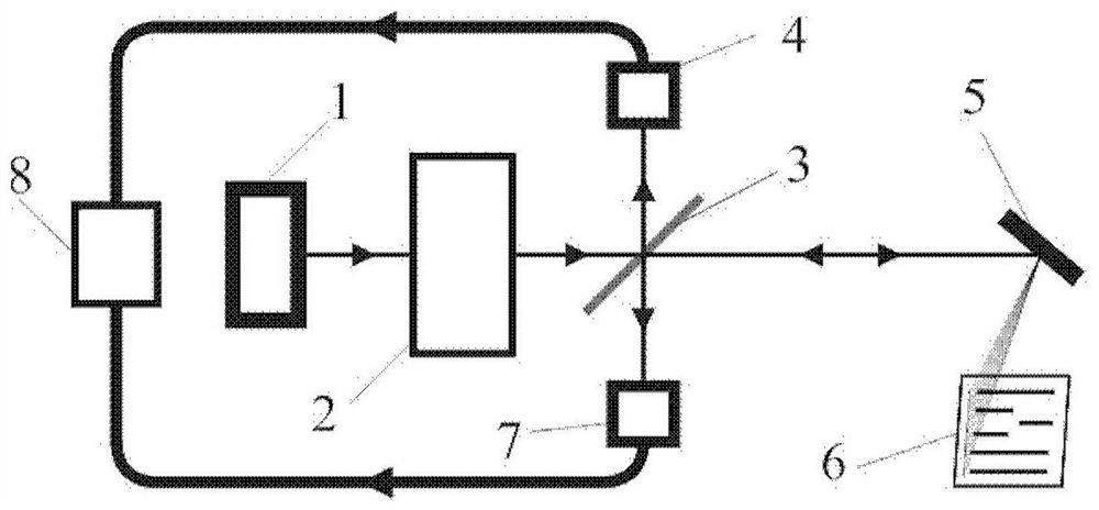
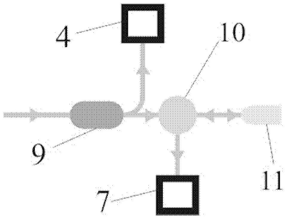
[0037] The invention uses a wide-spectrum optical frequency comb as a measurement light source, and divides a wide-spectrum pulse into a series of narrow-spectrum sub-pulses through processing. The series of sub-pulses have different spectral segments and are arranged at equal intervals in the time domain according to spectral components. Use the diffraction element to convert the spectral distribution into a spatial distribution. The sub-pulses at different spatial positions are reflected by the sample to be tested and return to the detector at different times. Using a single-pixel detector can complete multi-point measurement. According to the sub-pulse time-of-flight data can be Obtain 3D profile information. The device can be used to measure the surface contour of micro-nano devices, and is expected to provide a new detection method for the semiconductor field.

[0038] Specifically, the present invention discloses a device for measuring the surface contour of a micro-nano...


PUM


Abstract

A device for measuring the surface contour of a micro-nano device based on an optical frequency comb, including an optical frequency comb used as a measurement light source to output a wide-spectrum pulse; a pulse processing module used to pre-process the wide-spectrum pulse output by the optical frequency comb Add chirp and spectrum segmentation to process wide-spectrum pulses into a series of narrow-spectrum sub-pulses; half-mirrors are used to divide narrow-spectrum sub-pulses into reference light and signal light; diffraction elements are used to diffract signal light and convert The spectral distribution is converted into spatial distribution; the signal light detector is used to collect the signal light reflected by the sample to be measured and passed through the diffraction element and the half mirror. The measurement can be completed by using a single-pixel camera, which reduces the requirements on the detector pixels. The lateral resolution of profile measurement can be improved by increasing the number of sub-pulses, increasing the pulse repetition frequency and adjusting the translation speed of the device under test. The measurement speed is fast, and it can be used for surface profile measurement of micro-nano devices on the production line, meeting the requirements of high-throughput measurement.

Description

technical field [0001] The invention relates to the technical field of micro-nano profile measurement, in particular to a device and method for measuring the surface profile of a micro-nano device based on an optical frequency comb. Background technique [0002] Micro-nano device surface profile measurement technology has a wide range of applications in integrated circuits, MEMS devices and other fields. With the rapid development of microelectronics manufacturing technology and processing technology, the production efficiency of micro-nano devices is getting higher and higher, the structure is more and more complex, and the feature size is getting smaller and smaller, which requires high-resolution and rapid measurement of the surface profile of micro-nano devices presented new challenges. [0003] Among the traditional measurement methods, the contact measurement method has extremely high measurement accuracy and lateral resolution, but this type of method requires point-...

Claims


Application Information

Patent Timeline
Patent Type & Authority Patents(China)
IPC IPC(8): G01B11/24B82Y35/00
CPCG01B11/24B82Y35/00
Inventor 石俊凯李冠楠陈晓梅黎尧刘立拓高超董登峰周维虎
Owner INST OF MICROELECTRONICS CHINESE ACAD OF SCI
Why Eureka
Try Eureka