Supercharge Your Innovation With Domain-Expert AI Agents!

A method and system for laser chip integration testing

A test system and laser technology, which is applied in the direction of electronic circuit test, instrument, measurement circuit, etc., to achieve the effect of reducing human intervention, improving equipment utilization, improving test efficiency and test automation

Active Publication Date: 2021-03-02
上海菲莱测试技术有限公司
View PDF15 Cites 0 Cited by
  • Summary
  • Abstract
  • Description
  • Claims
  • Application Information

AI Technical Summary

Problems solved by technology

[0005] The embodiment of the present application provides a method for integrated testing of laser chips, which solves the traditional technical problems of requiring two devices for testing requirements and requiring human intervention for testing, thereby improving equipment utilization and laser chip testing efficiency. and the degree of test automation to reduce the technical effect of human intervention

Method used


Image

  • A method and system for laser chip integration testing
  • A method and system for laser chip integration testing
  • A method and system for laser chip integration testing

Examples


Embodiment 1

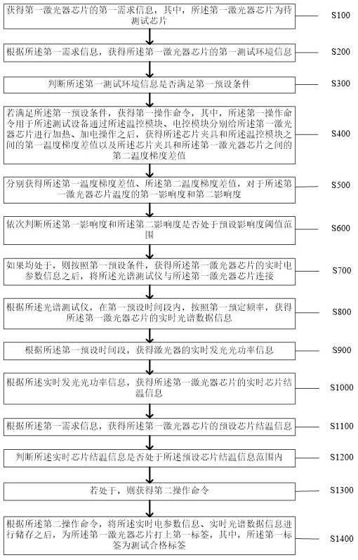
[0022] Such as figure 1 As shown, the embodiment of the present application provides a method for laser chip integration testing, which is applied to an intelligent test system, and the intelligent test system has a test device, and the test device has a temperature control module, an electrical control module and chip fixture, and the test equipment is connected to a spectrum tester in communication, wherein the method includes:

[0023] Step S100: Obtain first requirement information of a first laser chip, wherein the first laser chip is a chip to be tested;

[0024]Specifically, the first laser chip is a chip to be tested, a laser, and a device capable of emitting laser light. According to the working medium, lasers can be divided into gas lasers, solid-state lasers, semiconductor lasers, and dye lasers. The first requirement The information is various parameter information, working environment, temperature and other information of the first laser chip.

[0025] Step S200...

Embodiment 2

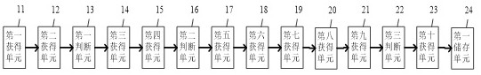
[0094] Based on the same inventive concept as a method for laser chip integration testing in the foregoing embodiments, the present invention also provides a system for laser chip integration testing, such as figure 2 As shown, the system includes:

[0095] The first obtaining unit 11: the first obtaining unit 11 is used to obtain the first requirement information of the first laser chip, wherein the first laser chip is a chip to be tested;

[0096] The second obtaining unit 12: the second obtaining unit 12 is configured to obtain the first test environment information of the first laser chip according to the first requirement information;

[0097] The first judging unit 13: the first judging unit 13 is used to judge whether the first test environment information satisfies a first preset condition;

[0098] The third obtaining unit 14: if the first preset condition is satisfied, the third obtaining unit 14 is used to obtain the first operation command, wherein the first oper...

Embodiment 3

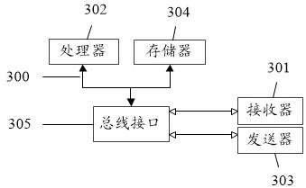
[0141] Refer below image 3 An electronic device according to an embodiment of the present application will be described.

[0142] image 3 A schematic structural diagram of an electronic device according to an embodiment of the present application is shown.

[0143] Based on the inventive idea of ​​a method for laser chip integration testing in the foregoing embodiments, the present invention also provides a system for laser chip integration testing, on which a computer program is stored, and the program is implemented when the program is executed by a processor. Steps in any one of the above-mentioned methods for laser chip integration testing.

[0144] Among them, in image 3In, bus architecture (represented by bus 300), bus 300 may include any number of interconnected buses and bridges, bus 300 will include one or more processors represented by processor 302 and various types of memory represented by memory 304 circuits linked together. The bus 300 may also link toget...


PUM


Abstract

The invention discloses a method and system for laser chip integration testing. The method includes: obtaining first requirement information and first test environment information of a first laser chip; judging whether the first test environment information satisfies the first predetermined Set the conditions; if the first operation command is satisfied, obtain the first and second influence degrees of the first and second temperature gradient differences on the temperature of the first laser chip respectively; determine whether the first and second influence degrees are within the preset influence degree threshold range ; If they are all in, connect the spectrum tester to the first laser chip; obtain the real-time spectral data information of the first laser chip; obtain the real-time chip junction temperature information and preset chip junction temperature information of the first laser chip; judge the real-time chip junction temperature information; Whether the temperature information is within the range of the preset chip junction temperature information; if so, the second operation command is obtained. It solves the traditional technical problems of requiring two devices to conduct demand testing and requiring human intervention testing.

Description

technical field [0001] The invention relates to the technical field of chip testing, in particular to a method and system for laser chip integration testing. Background technique [0002] As the demand for Internet and multimedia communication continues to grow, the demand for network hardware also increases. Optical fiber communication is gradually used in network communication and other fields, and the development of optoelectronic devices such as laser chips is also maturing. Therefore, the testing of laser chips appears to be particularly important. [0003] However, in the process of realizing the technical solution of the invention in the embodiment of the present application, the inventor of the present application found that the above-mentioned technology has at least the following technical problems: [0004] The traditional testing of laser chips can only complete spectral testing, and cannot take into account the aging test requirements at the same time, and cann...

Claims


Application Information

Patent Timeline
Patent Type & Authority Patents(China)
IPC IPC(8): G01R31/28
CPCG01R31/2865G01R31/2875
Inventor 张华薛银飞黄河
Owner 上海菲莱测试技术有限公司
Features
  • R&D
  • Intellectual Property
  • Life Sciences
  • Materials
  • Tech Scout
  • Unparalleled Data Quality
  • Higher Quality Content
  • 60% Fewer Hallucinations
Learn More