Infrared radio frequency signal detector based on metasurface optical antenna and preparation method thereof
An optical antenna and radio frequency signal technology, applied in the field of signal detection, can solve the problems of large volume and slow wave band, and achieve the effect of small volume
- Summary
- Abstract
- Description
- Claims
- Application Information
AI Technical Summary
Problems solved by technology
Method used
Image
Examples
Embodiment 1
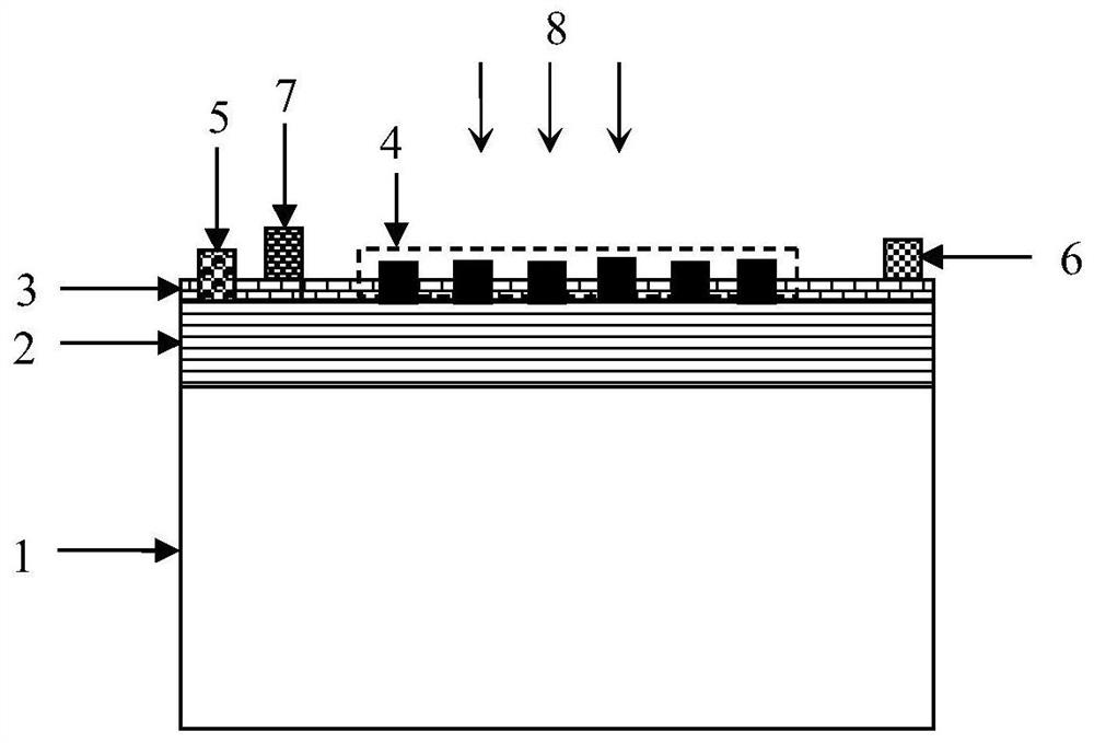
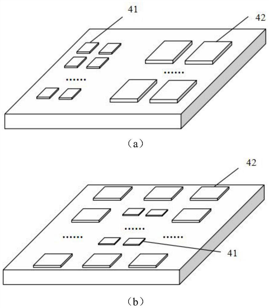
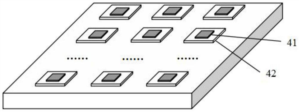
[0057] An infrared radio frequency signal detector based on a metasurface optical antenna, such as figure 1 As shown, it includes: substrate 1 (thickness 200-500μm), doped layer 2 (thickness 1um-2um, doping concentration 1×10 16 cm -3 ~9×10 18 cm -3 ) and a silicon dioxide layer 3 (thickness is 100-300nm), fabricated on the doped layer 2 and a metasurface optical antenna layer 4 (thickness is 50-220nm) that forms a Schottky contact with the doped layer 2, fabricated in On the doped layer 2, an ohmic electrode 5 forming an ohmic contact with the doped layer 2, and a Schottky electrode 6 and an ordinary electrode 7 positioned on the upper surface of the silicon dioxide layer 3; wherein, the metasurface optical antenna layer 4 is connected with the The Schottky electrode 6 is connected to the common electrode 7 , and its internal gap is filled with a silicon dioxide layer; the silicon dioxide layer 3 , the metasurface optical antenna layer 4 and the ohmic electrode 5 cover the...
Embodiment 2
[0065] An infrared radio frequency signal detector based on a metasurface optical antenna, such as Figure 9 As shown, it includes: a substrate 1, a first doped layer 12 and a first silicon dioxide layer 13 sequentially arranged upward from the upper surface of the substrate 1, a second doped layer 22 and a first silicon dioxide layer sequentially arranged downward from the lower surface of the substrate. The second silicon dioxide layer 23, the first metasurface optical antenna layer 14 formed on the first doped layer 12 to form a Schottky contact with the first doped layer 12, is made under the second doped layer 22 The second metasurface optical antenna layer 24 forming a Schottky contact with the second doped layer 22, the first ohmic electrode 15 formed on the first doped layer 12 and forming an ohmic contact with the first doped layer 12, making The second ohmic electrode 25 forming ohmic contact with the second doped layer 22 under the second doped layer 22, the first S...
Embodiment 3
[0074] A preparation method of the infrared signal detector provided by Embodiment 1 of the present invention, comprising the following steps:
[0075] S101. Implanting doping ions on the substrate (semi-insulating GaAs layer) by metal-organic compound chemical vapor deposition, with a doping concentration of 1×10 16 cm -3 ~9×10 18 cm -3 , forming a doped layer (N-type GaAs layer);
[0076] S102. Prepare a silicon dioxide layer on the doped layer by plasma-enhanced chemical vapor deposition, the thickness of which is 200nm-400nm;
[0077] S103. Photoetching the ohmic electrode contact hole pattern on the silicon dioxide layer through a positive resist process, and etching the silicon dioxide layer at the position of the ohmic electrode contact hole pattern to obtain an ohmic electrode contact hole; photolithography through a negative resist process Ohmic electrode pattern, using electron beam evaporation method to sequentially evaporate stacked Ni / Ge / Au layers (thicknesses...
PUM
| Property | Measurement | Unit |
|---|---|---|
| width | aaaaa | aaaaa |
| width | aaaaa | aaaaa |
| width | aaaaa | aaaaa |
Abstract
Description
Claims
Application Information
 - R&D
- Intellectual Property
- Life Sciences
- Materials
- Tech Scout
- Unparalleled Data Quality
- Higher Quality Content
- 60% Fewer Hallucinations
Browse by: Latest US Patents, China's latest patents, Technical Efficacy Thesaurus, Application Domain, Technology Topic, Popular Technical Reports.
© 2025 PatSnap. All rights reserved.Legal|Privacy policy|Modern Slavery Act Transparency Statement|Sitemap|About US| Contact US: help@patsnap.com


