Low-power LED lamp bead low-thermal-resistance packaging structure and packaging process

A technology of LED lamp beads and packaging structure, applied in electrical components, electric solid devices, circuits, etc., can solve the problems of cumbersome methods, difficult yield control, high temperature resistance, etc., to increase high refractive index and high light transmission. efficiency, easy disassembly and reuse, good durability and heat resistance

Active Publication Date: 2021-01-22
SHENZHEN YULIANG OPTOELECTRONICS TECH
View PDF11 Cites 2 Cited by
  • Summary
  • Abstract
  • Description
  • Claims
  • Application Information

AI Technical Summary

Problems solved by technology

[0003] The existing technology has the following disadvantages: the electro-optical conversion efficiency of the existing LED is about 20% to 30%, and 70% to 80% of the energy is converted into heat energy that cannot be released by radiation. If the heat dissipation of the package is not good, the temperature of the chip will increase , resulting in uneven stress distribution, reduced chip luminous efficiency, and reduced phosphor conversion efficiency
[0004] At present, the COB packaging process commonly used in the industry is as follows: First, use dam glue on the surface of the substrate that has not been bonded to the bonding wire along the edge of the bonding wire area. The purpose of the dam is to prevent the fluorescent colloid from flowing out during the subsequent sealing process. , play the role of blocking glue, and finally seal the fluorescent glue. The fluorescent powder has a great influence on the attenuation of white light and is not suitable for low-power LED lamp beads. Low, more labor input, and difficult to control the yield rate

Method used


Image

  • Low-power LED lamp bead low-thermal-resistance packaging structure and packaging process
  • Low-power LED lamp bead low-thermal-resistance packaging structure and packaging process
  • Low-power LED lamp bead low-thermal-resistance packaging structure and packaging process

Examples


Embodiment 1

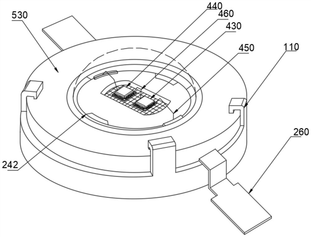
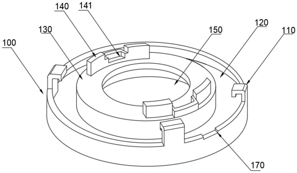
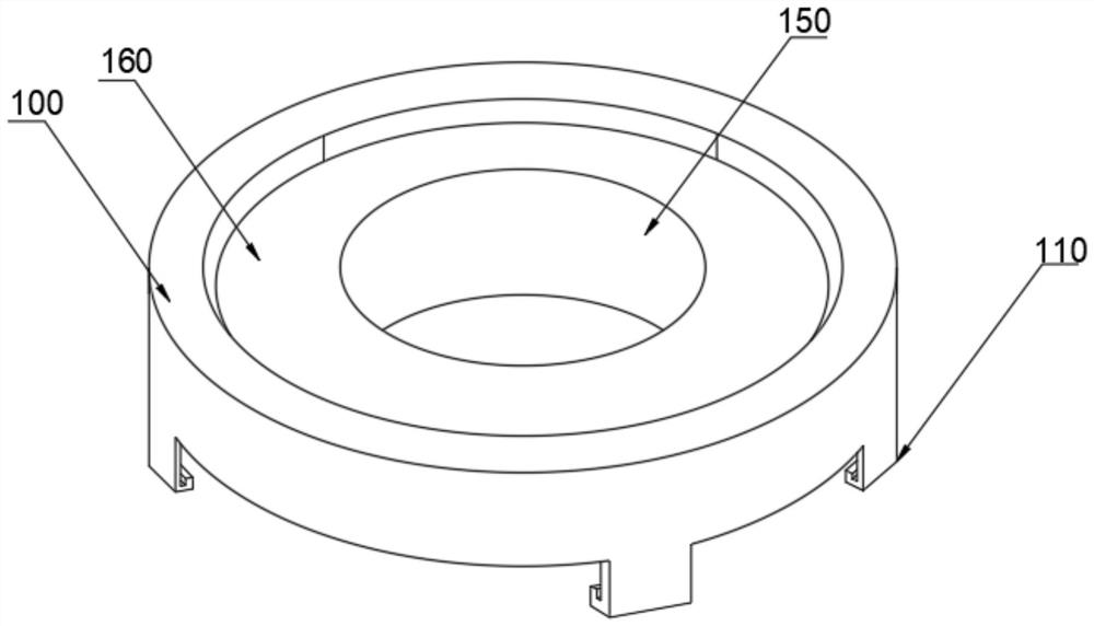
[0049] Embodiment 1, with reference to attached Figure 1-15 , a low thermal resistance packaging structure for low-power LED lamp beads provided by the present invention, including a base 100, a support base 200, a heat conduction device 300, a light-emitting component 400, an insulating sleeve 500 and a protection component 600, and the top of the base 100 is provided with a mounting groove 120 Specifically, the inner wall of the installation groove one 120 is provided with a support seat 200, the support seat 200 includes a chassis 210, the top of the chassis 210 is fixedly installed with a boss two 220, and the top of the boss two 220 is fixedly installed with a pad seat 230, and the pad seat 230 The top is provided with a cutting surface 232, the pad seat 230 is provided with a slot one 231 on both sides, and the inner wall of the slot one 231 is plugged with an electrode pin 260, and one end of the electrode pin 260 is fixedly installed on the inner wall of the cutting su...

Embodiment 2

[0061] A low-power LED lamp bead packaging process with low thermal resistance, the operating steps are:

[0062] Step 1: Ultrasonic cleaning of base 100, support base 200, heat conduction device 300 and insulating sleeve 500, and drying to remove moisture;

[0063] Step 2: Insert the chassis 210 into the inner wall of the installation slot 120, rotate the support base 200 so that the bump 140 and the groove 141 are clamped on the inner wall of the slot 2 250 and the bump 3 251, insert the pad 310 and the copper pillar 320 On the inner wall of the through hole 240, the pad 310 is installed on the top of the retaining ring 241, adjust the position of the pad 310 so that the groove 2 312 is engaged with the bump 242, and insert one end of the two sets of electrode pins 260 into the inner wall of the slot 1 231 , fixed at the connection between the cut surface 232 and the pad 310, and the bottom end of the electrode pin 260 is installed in the slot two 270 and the slot one 170 fo...

Embodiment 3

[0071] Refer to the attached Figure 16 , a low thermal resistance packaging structure of a low-power LED lamp bead in this embodiment, further comprising an aluminum column 370;

[0072] Further, the bottom of the copper column 320 is provided with a mounting groove 321, and the inner wall of the mounting groove 321 is fixed with an aluminum column 370. Specifically, the mounting groove 321 has a limiting effect on the aluminum column 370, and the aluminum column 370 has a positioning effect on the copper column 320. The effect of heat conduction efficiency and heat dissipation, the aluminum column 370 has good thermal conductivity and is not easy to rust and has the effect of reducing production cost.

[0073] The specific implementation scenario is: when using the present invention, workers in the field need to replace the aluminum pillars 370 with copper pillars 320 .


PUM


Abstract

The invention discloses a low-power LED lamp bead low-thermal-resistance packaging structure and a packaging process. The structure comprises a base, a supporting base, a heat conduction device, a light-emitting assembly, an insulating sleeve and a protection assembly, wherein a first mounting groove is formed in the top of the base, the supporting base is arranged on the inner wall of the first mounting groove, and the supporting base comprises a base plate; a second boss is fixedly installed at the top of the base plate, a bonding pad base is fixedly installed at the top of the second boss,a tangent plane is arranged at the top of the bonding pad base, first inserting grooves are formed in the two sides of the bonding pad base, electrode pins are inserted into the inner walls of the first inserting grooves, and one ends of the electrode pins are fixedly installed on the inner wall of the tangent plane. The invention has the beneficial effects that the fourth installation groove is formed in the bottom of the copper column, a heat conduction pipe is fixedly installed on the inner wall of the fourth installation groove, a fifth installation groove is formed in the inner wall of the heat conduction pipe, a heat conduction column is fixedly installed on the inner wall of the fifth installation groove, first ribs are evenly installed on the outer wall of the heat conduction pipeand the outer wall of the heat conduction column, and gaps between the first ribs are filled with heat dissipation silica gel, so the effect of releasing heat energy is achieved.

Description

technical field [0001] The invention relates to the technical field of LED lamp bead packaging, in particular to a low-power LED lamp bead packaging structure and packaging process with low thermal resistance. Background technique [0002] Due to its small size, full solid state, long life, environmental protection, power saving and other advantages, LED has been widely used in light source modules such as automotive lighting, decorative lighting, mobile phone flashlights, large and medium-sized NBs, LCD-TVs, etc. One of the most promising high-tech fields, green lighting with the advantages of energy saving, long life, maintenance-free, easy control, and environmental protection. As a new generation of green light source, high luminous efficiency is an essential feature of low-power LEDs. [0003] The existing technology has the following disadvantages: the electro-optical conversion efficiency of the existing LED is about 20% to 30%, and 70% to 80% of the energy is convert...

Claims


Application Information

Patent Timeline
Patent Type & Authority Applications(China)
IPC IPC(8): H01L33/64H01L33/62H01L33/48H01L25/075
CPCH01L25/0753H01L33/486H01L33/62H01L33/641H01L33/642H01L33/648H01L2933/0033H01L2933/0066H01L2933/0075
Inventor 尚五明
Owner SHENZHEN YULIANG OPTOELECTRONICS TECH
Why Eureka
Try Eureka