
Low-power-consumption high-performance super-junction JBS diode and manufacturing method thereof

A super-junction, high-performance technology, applied in semiconductor/solid-state device manufacturing, electrical components, circuits, etc., can solve the problems of difficult process, unfavorable promotion, high cost, etc., and achieve simple manufacturing process, low manufacturing cost and high durability Effect

Pending Publication Date: 2021-01-29
SHENYANG POLYTECHNIC UNIV
View PDF0 Cites 3 Cited by
  • Summary
  • Abstract
  • Description
  • Claims
  • Application Information

AI Technical Summary

Problems solved by technology

[0005] The present invention proposes a low-power-consumption high-performance super-junction JBS diode and its manufacturing method, which are manufactured using traditional techniques, and its purpose is to solve the problem of high power consumption, difficult process, high cost and unfavorable popularization in the existing power diode production technology The problem

Method used


Image

  • Low-power-consumption high-performance super-junction JBS diode and manufacturing method thereof
  • Low-power-consumption high-performance super-junction JBS diode and manufacturing method thereof
  • Low-power-consumption high-performance super-junction JBS diode and manufacturing method thereof

Examples


Embodiment Construction

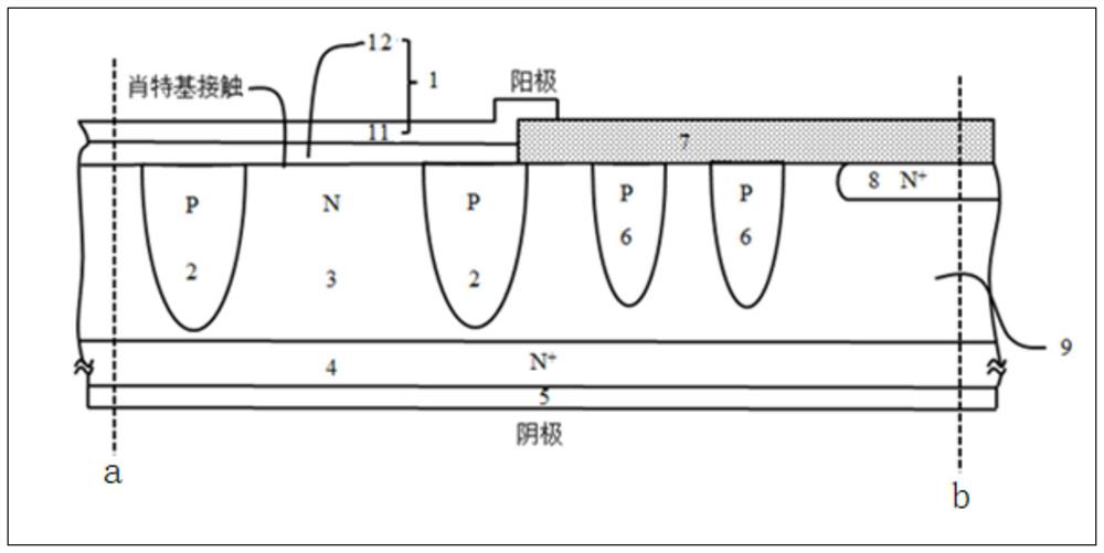
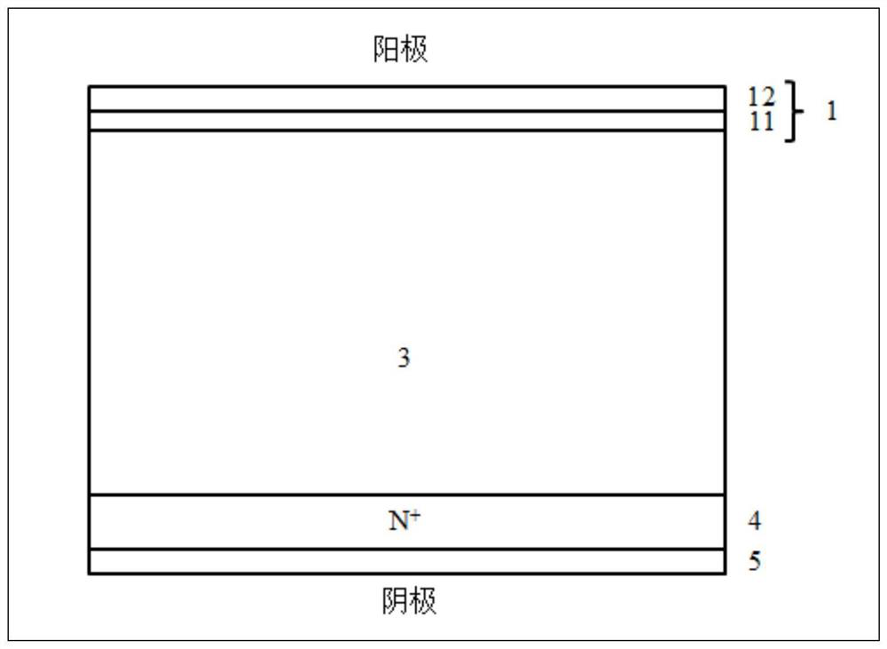
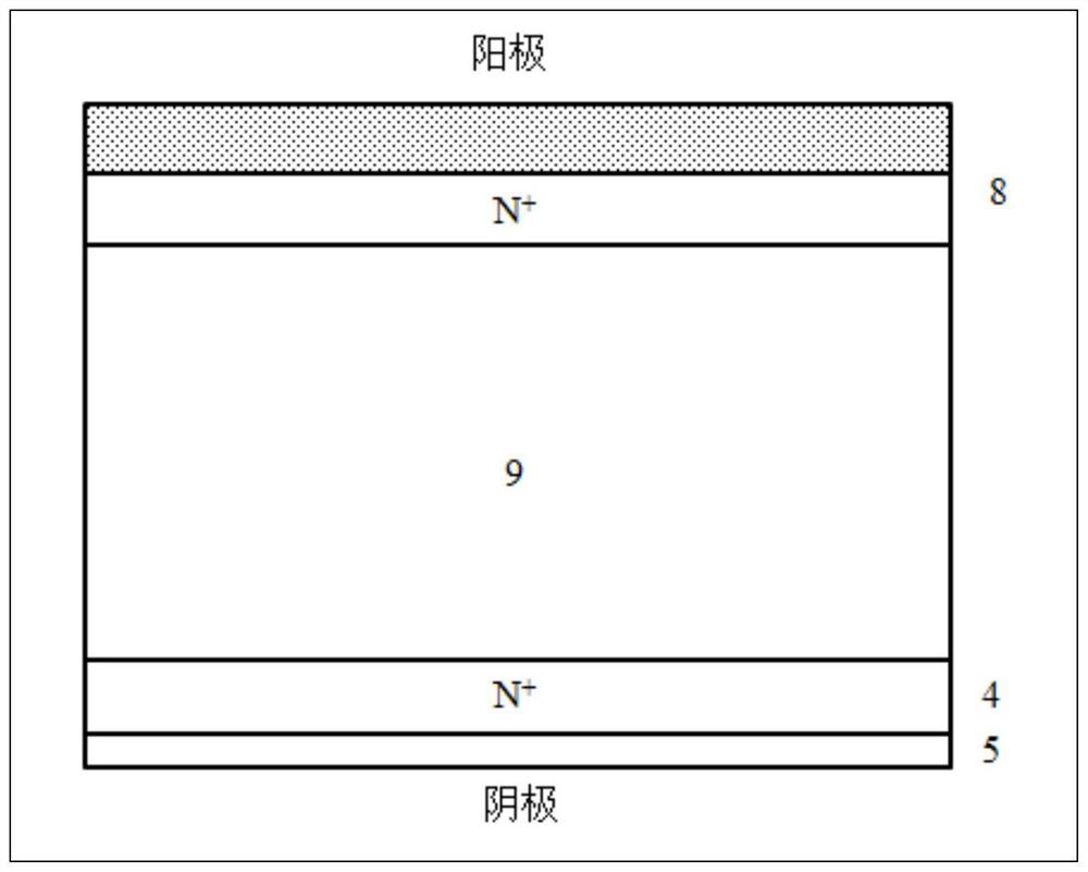
[0054] A low-power-consumption high-performance super-junction JBS diode includes: 1. Anode metal electrode; 11. Metal silicide layer; 12. Metal layer structure; 2. P heavily doped columnar region; 3. N columnar drift region; 4. N+ heavily doped region at the bottom; 5. Cathode metal electrode; 6. P-type field effect ring; 7. Insulation barrier layer; 8. N+ type stop ring; 9. Terminal.

[0055] Low power consumption and high performance super-junction JBS diodes use high-concentration N+ doped silicon wafers as the overall substrate of the device, and this high-concentration wafer becomes the N+ heavily doped region 4 at the bottom of the device after the device is integrally formed. The bottom N+ heavily doped region 4 is connected to the metal electrode by means of ohmic contact, and the metal electrode connected below the bottom N+ heavily doped region 4 is the cathode metal electrode 5 of the device. The function of connecting the cathode electrode can also support the dev...


PUM

PropertyMeasurementUnit
Thicknessaaaaaaaaaa

Abstract

The invention belongs to the field of power semiconductor devices, and particularly relates to a low-power-consumption high-performance super-junction JBS diode and a manufacturing method thereof. Thelow-power-consumption high-performance super-junction JBS diode is manufactured by using a traditional silicon-based process technology, so that the manufacturing cost is low; a P heavily doped cylindrical region and an N cylindrical drift region which have the characteristics of large area, high concentration and large junction depth are adopted, so that the forward conduction resistance is reduced; a super junction is formed, and good reverse blocking characteristics are achieved by optimizing electric field distribution; by optimizing parameters of the super junction, higher blocking withstand voltage can be realized, and the on-state and off-state power consumption of the device is reduced; and optimal two-dimensional electric field distribution is obtained by optimizing the doping concentration and width of the P column region and the N column region, unification of high blocking voltage and low on-resistance and unification of high blocking voltage and rapid switching are achieved, compromise between forward on-state voltage drop and reverse blocking characteristics and compromise between reverse recovery characteristics and reverse blocking voltage are optimized, and the limit of a traditional silicon material is broken through.

Description

Technical field: [0001] The invention belongs to the field of power semiconductor devices, and relates to a low-power-consumption high-performance super junction JBS diode and a manufacturing method thereof. Background technique: [0002] In modern power circuits, switching devices are often used to regulate the flow of power to the load and power diodes are used to control the direction of the current. With the emergence of high-performance power switching devices, such as power metal-oxide-semiconductor field-effect transistors (Metal-Oxide-Semiconductor Field-Effect Transistor) and insulated gate bipolar transistors (InsulatedGate Bipolar Transistor), the performance of power diodes has become a limiting power circuit major factor in performance. For example, the large reverse recovery current of traditional power diodes not only increases the power consumption of itself, but also increases the power consumption of switching devices, which affects the overall performance...

Claims


Application Information

Patent Timeline
IPC IPC(8): H01L29/06H01L29/872H01L21/329
CPCH01L29/872H01L29/66143H01L29/0634
Inventor 关艳霞刘勇刘斌刘桐
Owner SHENYANG POLYTECHNIC UNIV
Learn More