Biosensor based on graphene field effect transistor and preparation method and application thereof
A technology of field-effect transistors and biosensors, applied in the field of biosensors, can solve problems such as application limitations and electrical sensitivity limitations, and achieve the effects of rapid response, stable performance, and high detection limit
- Summary
- Abstract
- Description
- Claims
- Application Information
AI Technical Summary
Problems solved by technology
Method used
Image
Examples
preparation example Construction
[0036] In a second aspect, the present invention also provides a method for preparing a biosensor based on a graphene field effect transistor, comprising the following steps:
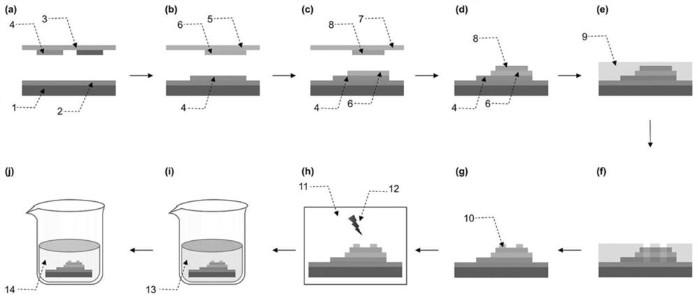
[0037] Fabrication of graphene / boron nitride / graphene van der Waals heterojunction: provide graphene, hexagonal boron nitride nanosheets, and single-throw silicon oxide sheets, attach graphene to a silicon dioxide spacer to obtain graphene Gate electrode, and then transfer the hexagonal boron nitride nanosheets to the graphene gate electrode to obtain the hexagonal boron nitride gate oxide layer, and finally transfer the graphene to the hexagonal boron nitride gate oxide layer to obtain the graphene channel. Obtain graphene / boron nitride / graphene van der Waals heterojunction;
[0038] Preparation of biosensors based on graphene field-effect transistors: source and drain electrodes are deposited on graphene channels of graphene / boron nitride / graphene van der Waals heterojunctions to obtain two-dimensiona...
Embodiment 1
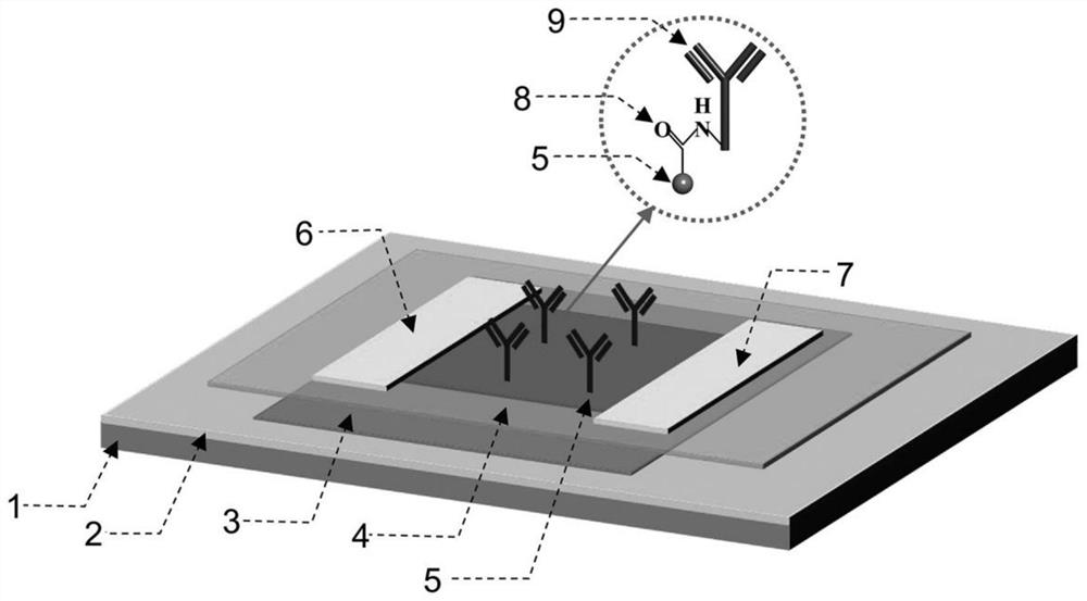
[0054] Such as figure 1 Shown is a graphene-based field-effect transistor biosensor. The graphene field-effect transistor-based biosensor has a p-type doped silicon substrate 1, a silicon dioxide isolation layer 2, a mechanically exfoliated graphene gate electrode 3, and a mechanically exfoliated hexagonal boron nitride gate oxide from bottom to top. Layer 4, mechanically exfoliated graphene channel 5, source electrode 6, drain electrode 7, activated carboxyl groups 8 on the surface of graphene channel, and the specificity associated with the occurrence and development of Alzheimer's disease (hereinafter referred to as "AD") Antibody 9.
[0055] Further, the thickness of the silicon substrate is 300 μm, and the resistivity is 2Ω·cm.
[0056] Further, the thickness of the silicon dioxide isolation layer is 300nm.
[0057] Further, graphene is single-atom thick.
[0058] Further, the thickness of the hexagonal boron nitride is 23nm.
[0059] Further, the source and drain el...
Embodiment 2
[0071] Identical to the structure of the biosensor based on the graphene field effect transistor in Example 1, the biosensor based on the graphene field effect transistor has a p-type doped silicon substrate 1, a silicon dioxide isolation layer 2, Mechanically exfoliated graphene gate electrode 3, mechanically exfoliated hexagonal boron nitride gate oxide layer 4, mechanically exfoliated graphene channel 5, source electrode 6, drain electrode 7, activated carboxyl groups 8 on the surface of graphene channel, and AD generation 9. Development of related specific antibodies.
[0072] Further, the silicon substrate has a thickness of 500 μm and a resistivity of 10 Ω·cm.
[0073] Further, the thickness of the silicon dioxide isolation layer is 500nm.
[0074] Further, graphene is single-atom thick.
[0075] Further, the thickness of the hexagonal boron nitride is 28nm.
[0076] Further, the source and drain electrodes are made of chromium / gold material, wherein the thickness of ...
PUM
| Property | Measurement | Unit |
|---|---|---|
| thickness | aaaaa | aaaaa |
| electrical resistivity | aaaaa | aaaaa |
| thickness | aaaaa | aaaaa |
Abstract
Description
Claims
Application Information


